Lead structures with vertical offsets

a technology of vertical offset and lead structure, applied in the direction of semiconductor devices, semiconductor/solid-state device details, electrical apparatus, etc., can solve the problems of increasing the height of the structure, impairing the signal transmission of adjacent signals, and posing significant problems in the lead conductance, so as to reduce the mutual inductance and increase the structure height

Inactive Publication Date: 2015-09-01
TESSERA INC
View PDF25 Cites 1 Cited by
  • Summary
  • Abstract
  • Description
  • Claims
  • Application Information

AI Technical Summary

Benefits of technology

[0010]As further discussed below, the vertical offset between sections of mutually-adjacent connectors provide increased distances between the adjacent connectors and reduced mutual inductance between adjacent connectors.
[0012]The structure desirably includes an elongated connectors extending between the first-row contact and the second-row contact of each of the single-connection pairs, the connectors associated with the first pairs being low connectors, the connectors associated with the second pairs being high connectors. In a structure according to this aspect of the invention, the high connectors desirably have at least about 30% of their length disposed above the second contacts, whereas the low connectors having at least about 30% of their length disposed below the second contacts. In certain embodiments a structure according to this aspect of the invention provide reduced mutual inductance without appreciably increasing the height of the structure.

Problems solved by technology

Inductances in the leads can pose significant issues.
This rapidly changing voltage effectively constitutes “noise” or unwanted voltage fluctuations on the adjacent lead and impairs signal transmissions on the adjacent lead.
These problems have become more significant as the speed of operation of components such as semiconductor chips has increased, and the frequency of signals sent along the leads has also increased.

Method used


Image

  • Lead structures with vertical offsets
  • Lead structures with vertical offsets
  • Lead structures with vertical offsets

Examples


Embodiment Construction

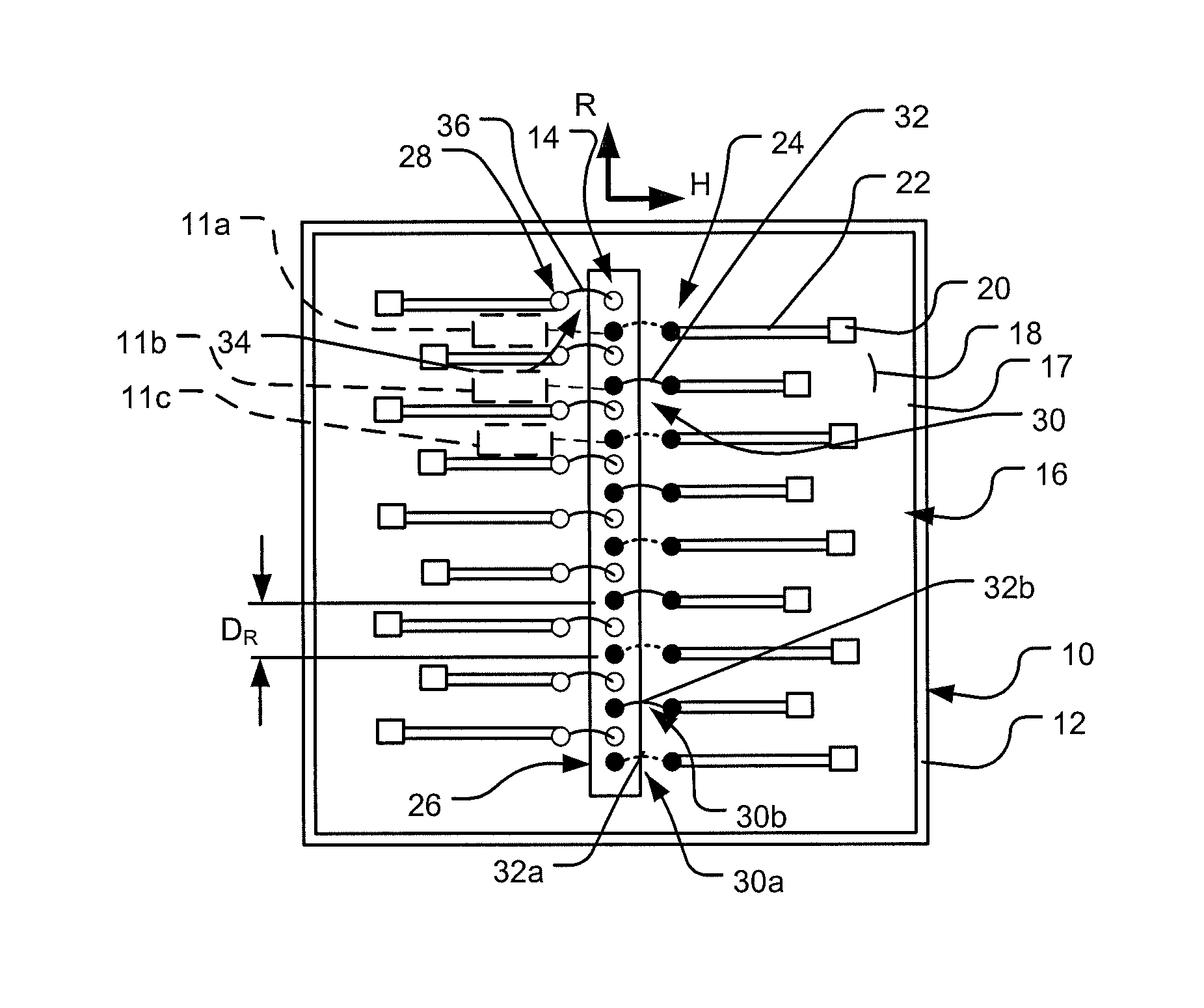
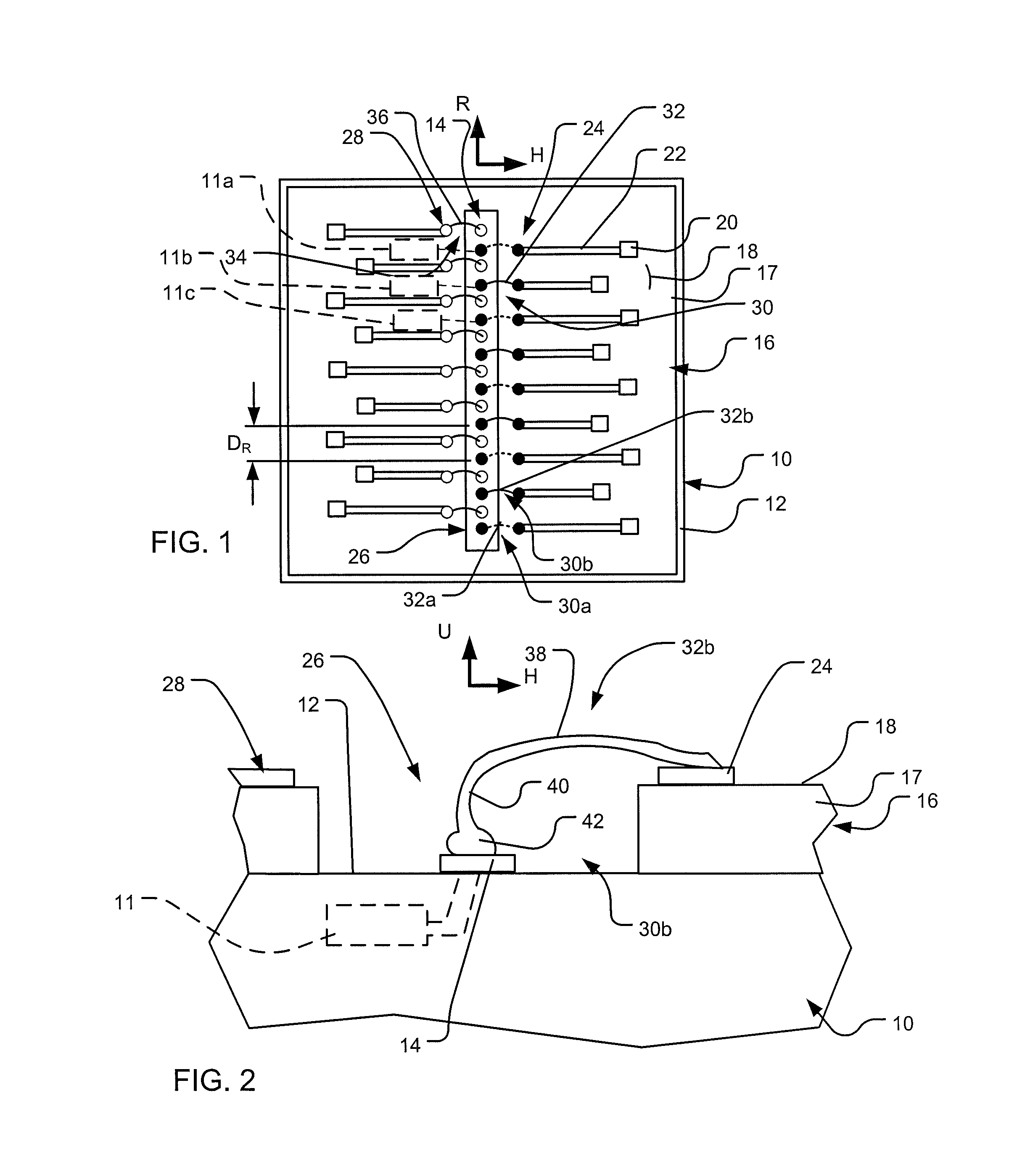
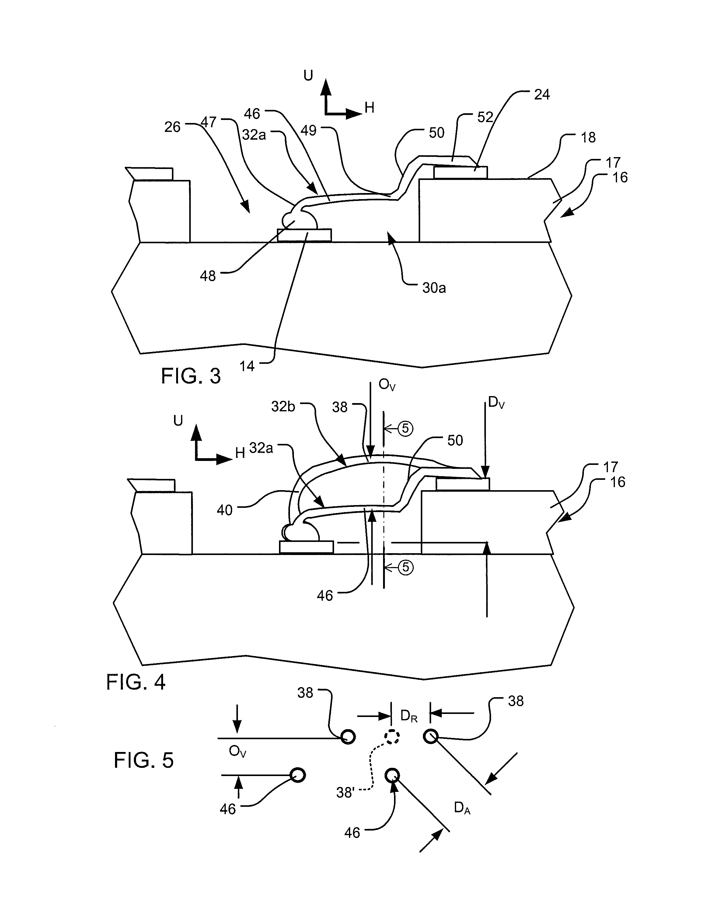
[0026]A structure in accordance with one embodiment of the invention includes a first element 10 in a form of a semiconductor chip having a front surface 12 facing toward the viewer in FIG. 1. The first element or chip 10 defines a first row of contacts 14 extending in a row direction R. The front surface 12 of the chip is generally planar, and contacts 14 are disposed in a first plane parallel to the plane of the front surface. For example, the contacts may be coplanar with the front surface, recessed from the front surface, or standing proud of the front surface 12. Chip 10 includes numerous internal circuits 11, only a few of which are depicted in FIGS. 1 and 2. Each contact 14 is connected to one or more of the internal circuits. Many or all of the contacts 14 are connected to different ones of the internal circuits 11. For example, one contact 14 is connected to internal circuit 11a (FIG. 1), another contact 14 is connected to internal circuit 11b and yet another contact 14 is ...


PUM


Abstract

A microelectronic structure includes a first row of contacts (14) and a second row of contacts (24) offset from the first row, so that the first and second rows cooperatively define pairs of contacts. These pairs of contacts include first pairs (30a) and second pairs (30b) arranged in alternating sequence in the row direction. The first pairs are provided with low connectors (32a), whereas the second pairs are provided with high connectors (32b). The high connectors and low connectors have sections vertically offset from one another to reduce mutual impedance between adjacent connectors.

Description

CROSS-REFERENCE TO RELATED APPLICATION[0001]The present application is a national phase entry under 35 U.S.C. §371 of International Application No. PCT / US2011 / 061647 filed Nov. 21, 2011, published in English, which claims the benefit of the filing date of U.S. Provisional Patent Application No. 61 / 416,779, filed Nov. 24, 2010. The disclosure of the foregoing are hereby incorporated herein by reference.FIELD OF THE INVENTION[0002]The present invention relates to microelectronic structures, leads for the same, and methods of forming microelectronic structures.BACKGROUND OF THE INVENTION[0003]Many microelectronic structures are made with rows of contacts interconnected with one another by leads such as wire bonds. For example, a microelectronic element such as a semiconductor chip may be made with one or more rows of contacts exposed at a front surface of the chip. Each row of contacts extends in a direction referred to herein as the “row direction.” A package substrate may overlie the...

Claims


Application Information

Patent Timeline
Patent Type & Authority Patents(United States)
IPC IPC(8): H01L23/495H01L23/13H01L23/00
CPCH01L23/49575H01L23/13H01L24/48H01L24/49H01L24/06H01L2224/06136H01L2224/45015H01L2224/4809H01L2224/4824H01L2224/48091H01L2224/48095H01L2224/48465H01L2224/49052H01L2224/49111H01L2224/49175H01L2224/49176H01L2924/01005H01L2924/01006H01L2924/01033H01L2924/01082H01L2924/1432H01L2924/1433H01L2924/1434H01L2924/20751H01L2924/3011H01L2924/30107H01L2924/00014H01L2924/00H01L2224/48227H01L2924/00012H01L2224/04042H01L2224/45099H01L2224/05599
Inventor CRISP, RICHARD DEWITTHABA, BELGACEMZOHNI, WAEL
Owner TESSERA INC
Why Eureka
Try Eureka