Semiconductor device and operation method thereof

a semiconductor device and operation method technology, applied in the field of semiconductor device and operation method thereof, can solve the problems of increasing the number of transfer lines for transferring delay control codes burden in layout design, etc., and achieve the effect of reducing the area of the semiconductor device and minimizing the configuration of the circuit for controlling the signal transfer characteristics of data

Active Publication Date: 2015-09-08
SK HYNIX INC
View PDF3 Cites 0 Cited by
  • Summary
  • Abstract
  • Description
  • Claims
  • Application Information

AI Technical Summary

Benefits of technology

[0020]The configuration of a circuit for controlling signal transfer characteristics of data may be minimized, resulting in a reduction of an area of the semiconductor device.

Problems solved by technology

An increase in the number of the first to nth delay control codes CTR1 to CTRn leads to an increase in the number of transfer lines for transferring the delay control codes, resulting in a burden in a layout design.
That is, when the bit number of the delay control codes is increased, the number of the long signal lines is also increased, resulting in a burden in the layout design.

Method used


Image

  • Semiconductor device and operation method thereof
  • Semiconductor device and operation method thereof
  • Semiconductor device and operation method thereof

Examples


Embodiment Construction

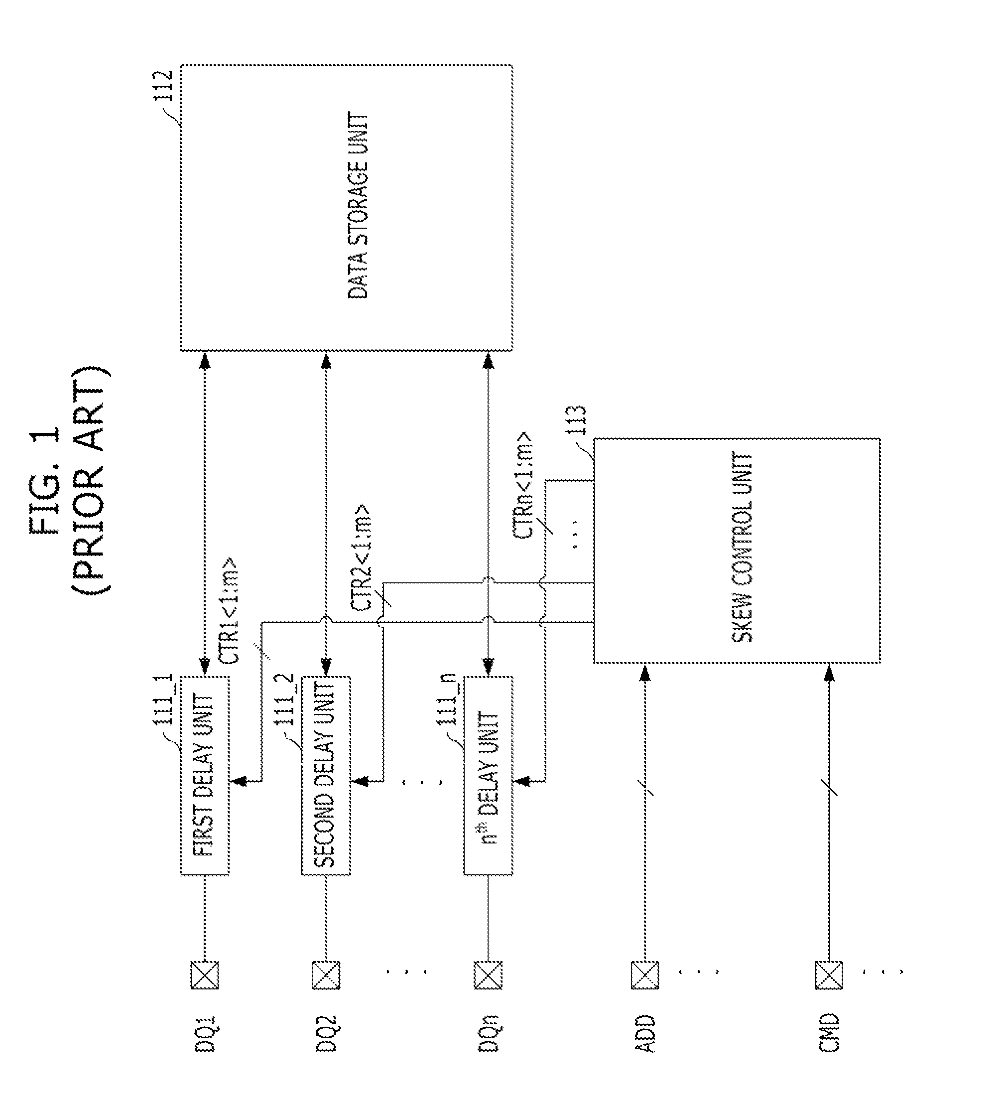
[0024]Exemplary embodiments of the present invention will be described below in more detail with reference to the accompanying drawings. The present invention may, however, be embodied in different forms and should not be construed as limited to the embodiments set forth herein. Rather, these embodiments are provided so that this disclosure will be thorough and complete, and will fully convey the scope of the present invention to those skilled in the art. Throughout the disclosure, like reference numerals refer to like parts throughout the various figures and embodiments of the present invention.

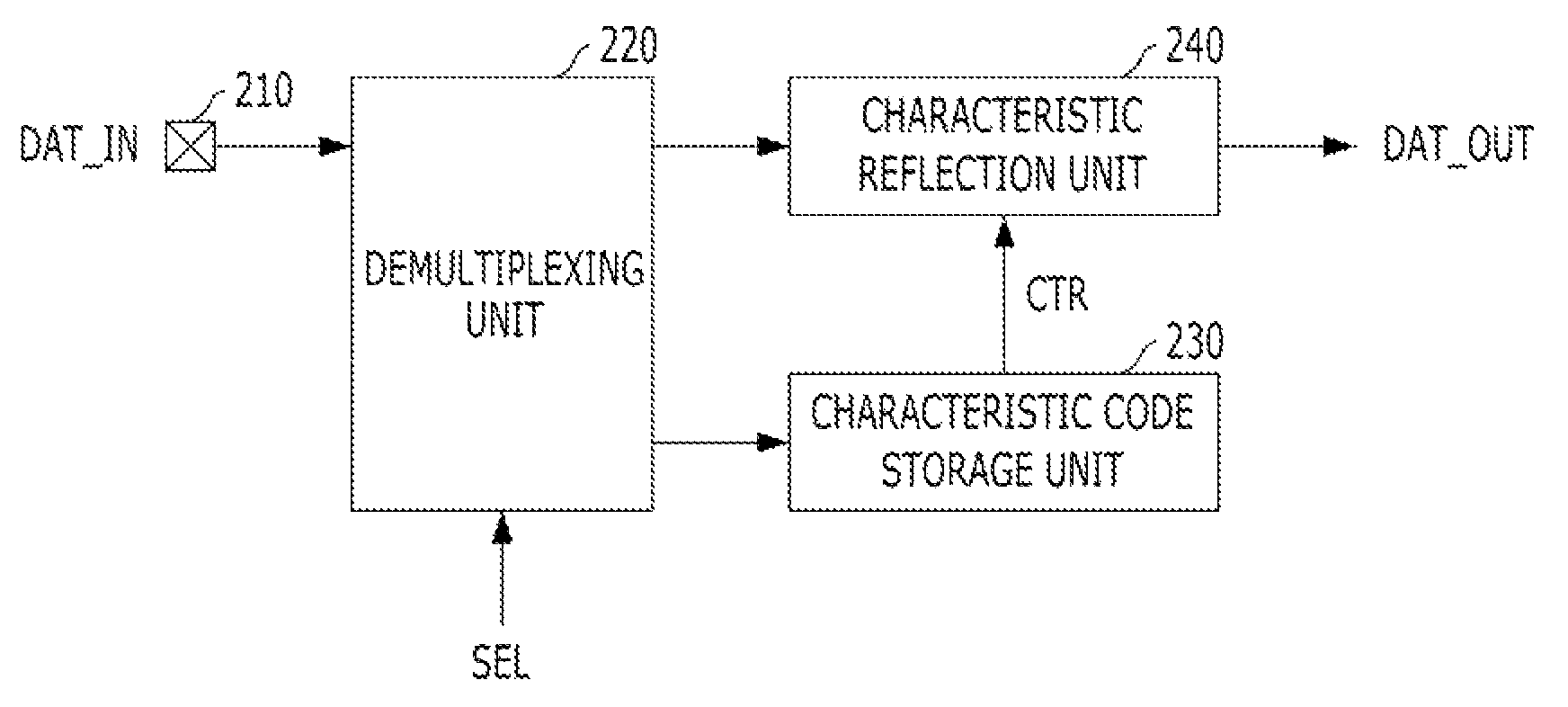
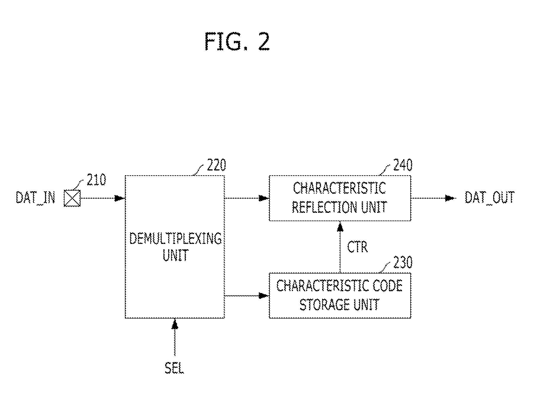
[0025]FIG. 2 is a block diagram illustrating a partial configuration of a semiconductor device in accordance with an embodiment of the present invention.

[0026]Referring to FIG. 2, the semiconductor device includes an input pad 210, a demultiplexing unit 220, a characteristic code storage unit 230, and a characteristic code reflection unit 240.

[0027]The demultipiexing unit 220 is configured t...


PUM


Abstract

A semiconductor device includes a characteristic code storage unit configured to store signal transfer characteristic information input through a given pad and output a control code corresponding to the signal transfer characteristic information, and a characteristic reflection unit configured to reflect the signal transfer characteristic information in an input signal input through the given pad, in response to the control code, and to output the reflected input signal.

Description

CROSS-REFERENCE TO RELATED APPLICATIONS[0001]The present application claims priority of Korean Patent Application No. 10-2012-0095049, filed on Aug. 29, 2012, which is incorporated herein by reference in its entirety.BACKGROUND[0002]1. Field[0003]Exemplary embodiments of the present invention relate to a semiconductor design technology, and more particularly, to a semiconductor device that controls skews of a plurality of input signals.[0004]2. Description of the Related Art[0005]In general, a semiconductor memory device such as a double data rate synchronous DRAM (DDR SDRAM) receives a plurality of signals such as commands, addresses, or data from an exterior, and performs a write operation or a read operation. In the write operation, the semiconductor memory device receives addresses and data and stores the data in a memory cell corresponding to the addresses. Furthermore, in the read operation, the semiconductor memory device outputs the data stored in the memory cell correspondi...

Claims


Application Information

Patent Timeline
Patent Type & Authority Patents(United States)
IPC IPC(8): G06F3/00G11C7/22G11C7/10G11C11/4076G11C11/4093G11C11/4096
CPCG06F3/00G11C7/109G11C7/1012G11C7/1066G11C7/1093G11C7/22G11C11/4076G11C11/4093G11C11/4096G11C7/10
Inventor CHOI, HAE-RANGKIM, YONG-JUKWON, DAE-HANJANG, JAE-MIN
Owner SK HYNIX INC
Why Eureka
Try Eureka