
Semiconductor device and electronic apparatus

a technology of semiconductor devices and electronic devices, applied in semiconductor devices, electrical devices, semiconductor/solid-state device details, etc., can solve the problem that normal-on field-effect transistors such as algan/gan hfet cannot be used in power devices, and cannot be used without. problem, to achieve the effect of reducing the loop area of the electric current path(s) and reducing the influence of the parasitic parameters of the package on the electrical characteristics

Active Publication Date: 2015-09-08
SHARP KK
View PDF6 Cites 4 Cited by
  • Summary
  • Abstract
  • Description
  • Claims
  • Application Information

AI Technical Summary

Benefits of technology

The present invention is a semiconductor device that reduces the area of the electrical current paths, which helps to improve the device's electrical performance. This also reduces the impact of external factors like the package design on the device's performance.

Problems solved by technology

This causes a problem that a normally-on field-effect transistor such as the AlGaN / GaN HFET cannot, without any alterations thereto, be used in a power device.

Method used


Image

  • Semiconductor device and electronic apparatus
  • Semiconductor device and electronic apparatus
  • Semiconductor device and electronic apparatus

Examples


embodiment 1

[0046]The following description will discuss Embodiment 1 of the present invention with reference to FIGS. 1 through 7.

[0047][Circuit Configuration (Operation) and Circuit Structure of Semiconductor Device]

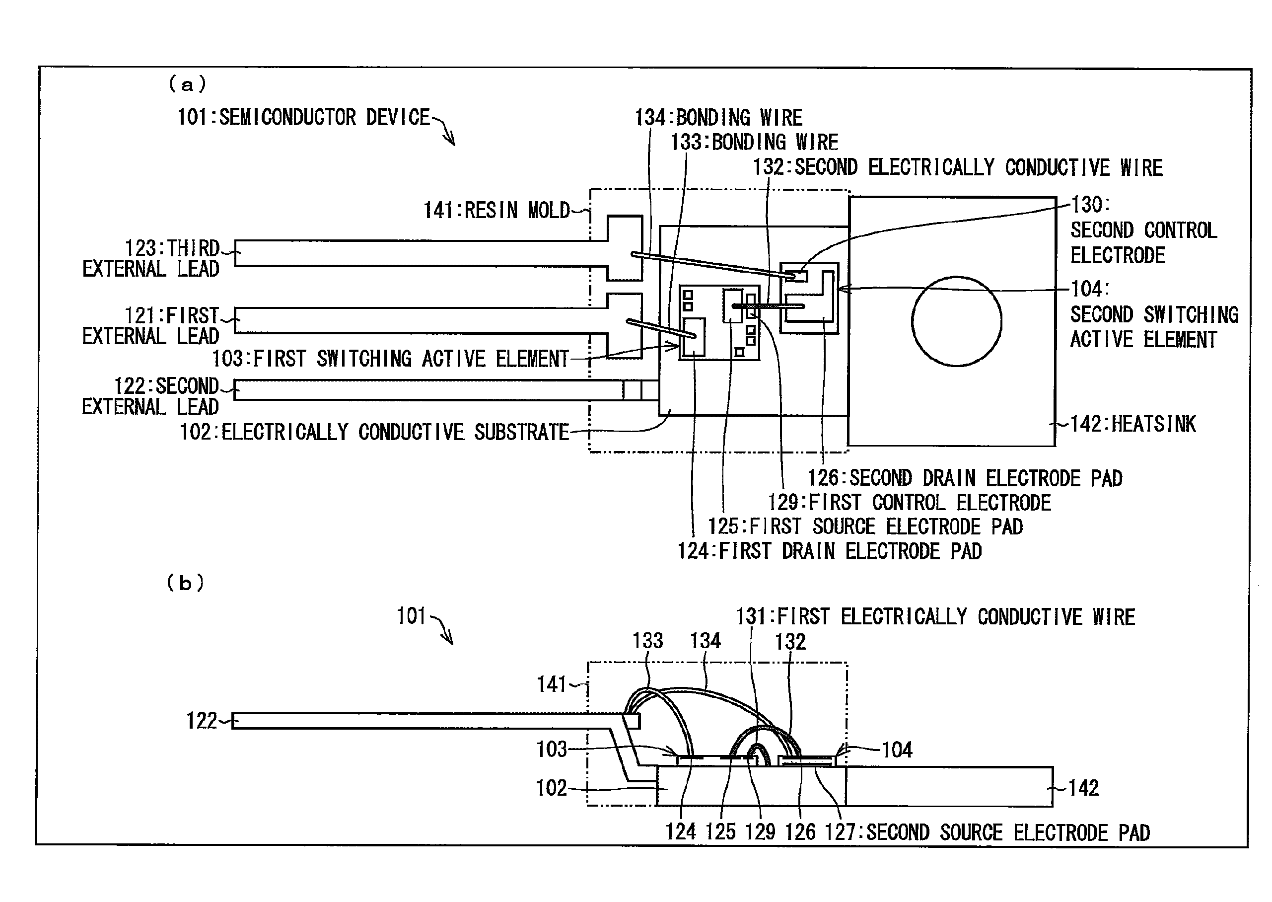
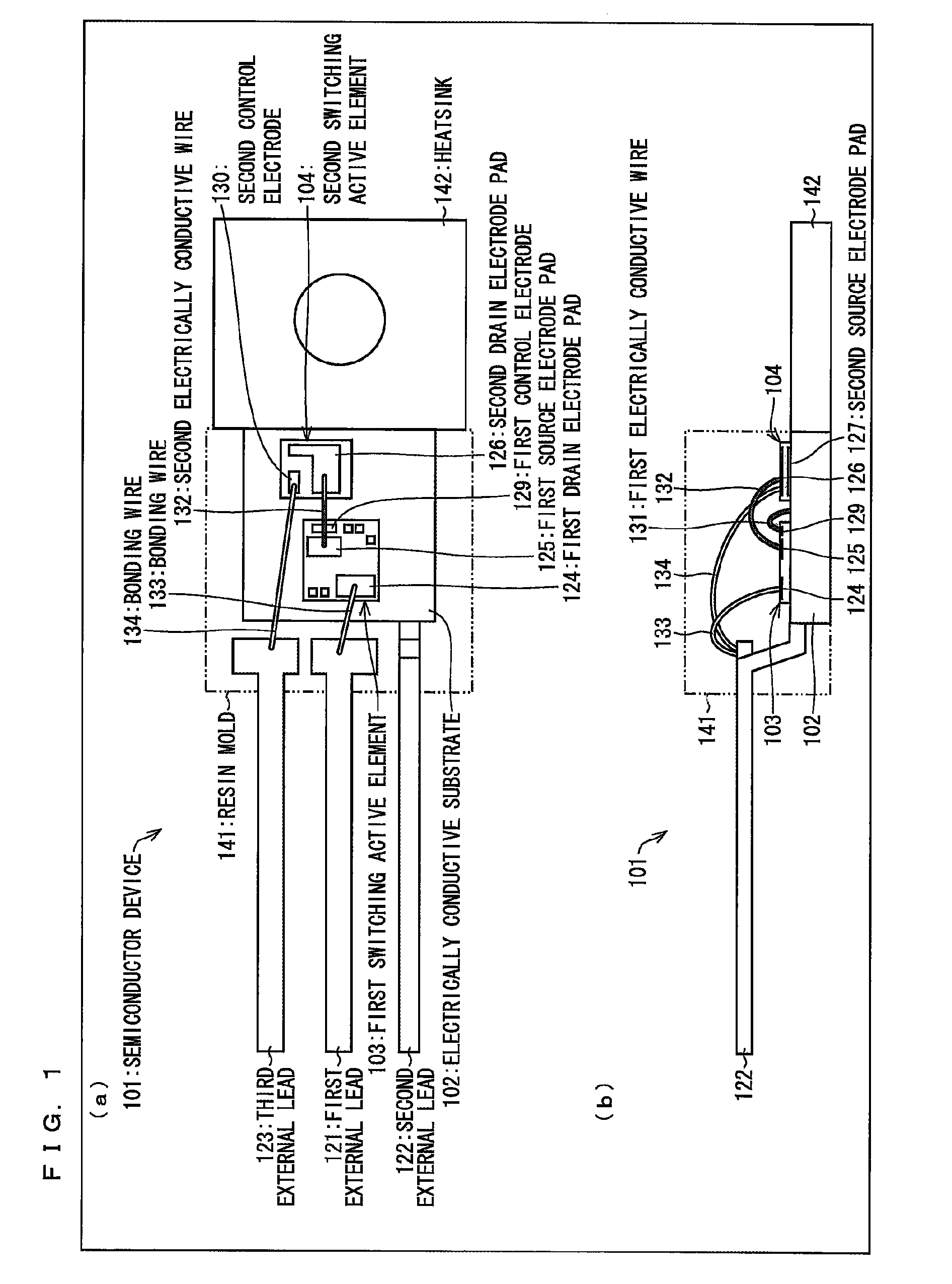
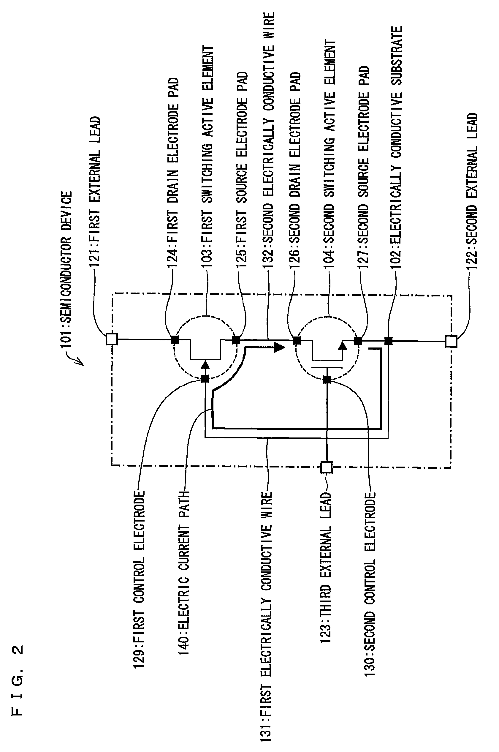
[0048](a) of FIG. 1 is a plan view illustrating a configuration of a semiconductor device 101 in accordance with Embodiment 1 of the present invention. (b) of FIG. 1 is a side view illustrating the configuration of the semiconductor device 101. FIG. 2 is a circuit diagram illustrating a circuit configuration of the semiconductor device 101.

[0049]As illustrated in (a) and (b) of FIG. 1, the semiconductor device 101 is configured by a TO220 package having three external leads. The semiconductor device 101 includes (i) an electrically conductive substrate 102, (ii) a first switching active element 103, (iii) a second switching active element 104, (iv) first through third external leads 121 through 123 (respectively), (v) first and second electrically conductive wires 131 and 132 (res...

embodiment 2

[0104]The following description will discuss Embodiment 2 of the present invention with reference to (a) and (b) of FIG. 8 and FIG. 10.

[0105](a) of 8 is a plan view illustrating a configuration of a semiconductor device 201 in accordance with Embodiment 2 of the present invention. (b) of FIG. 8 is a side view of the semiconductor device 201.

[0106]As is the case of the semiconductor device 101, the semiconductor device 201 is configured by a TO220 package (see (a) and (b) of FIG. 8). The semiconductor device 201 includes (i) an electrically conductive substrate 202, (ii) a first switching active element 203, (iii) a second switching active element 204, (iv) first through third external leads 221 through 223 (respectively), (v) a first electrically conductive wire 231, (vi) second electrically conductive wires 232a and 232b, (vii) bonding wires 233a and 233b, (viii) a bonding wire 234, (ix) a resin mold 241, and (x) a heatsink 242. Of these parts, the first through third external lead...

embodiment 3

[0124]The following description will discuss, with reference to (a) and (b) of FIG. 11 and FIG. 12, a semiconductor device in accordance with another embodiment.

[0125][Structure of Semiconductor Device]

[0126](a) of FIG. 11 is a plan view illustrating a configuration of a semiconductor device 401 in accordance with Embodiment 3 of the present invention. (b) of FIG. 11 is a side view illustrating the configuration of the semiconductor device 401. FIG. 12 is a circuit diagram illustrating a circuit configuration of the semiconductor device 401.

[0127]As illustrated in (a) of FIG. 11, the semiconductor device 401 is configured by a TO220 package including three external leads. The semiconductor device 401 includes (i) an electrically conductive substrate 402, (ii) a first switching active element 403, (iii) a second switching active element 404, (iv) first and second electrically conductive wire 431 and 432 (respectively), (v) bonding wires 433 and 434, (vi) a resin mold 441, and (vii) a...


PUM


Abstract

According to a semiconductor device (101), a first switching active element (103) of a normally-on type and a second switching active element (104) of a normally-off type are cascode-connected to each other. This causes an electric current path to be formed. The first and second switching active elements (103, 104) are provided and connected so that loop area of the electric current path is a minimum area in a plan view of the semiconductor device (101).

Description

[0001]This application is the U.S. national phase of International Application No. PCT / JP2012 / 074973 filed 27 Sep. 2012 which designated the U.S. and claims priority to JP Patent Application No. 2011-256685 filed Nov. 24, 2011 and JP Patent Application No. 2012-033036 filed 17 Feb. 2012, the entire contents of each of which are hereby incorporated by reference.TECHNICAL FIELD[0002]The present invention relates to (i) a semiconductor device including a normally-on switching active element and (ii) an electronic device (electronic apparatus) including the semiconductor device.BACKGROUND ART[0003]In light of a decrease in electric power consumption of home electric appliances, an emphasis has been placed on reducing power loss of semiconductors such as power devices and power modules. In view of the circumstances, semiconductor devices such as power devices employing wide bandgap semiconductors have been developed for the purpose of further reduction in power loss.[0004]Since field-eff...

Claims


Application Information

Patent Timeline
Patent Type & Authority Patents(United States)
IPC IPC(8): H01L21/02H01L27/088H01L23/495H01L29/20H01L23/00
CPCH01L27/0883H01L23/49562H01L23/49575H01L24/49H01L29/2003H01L2224/2919H01L2224/29139H01L2224/32245H01L2224/45124H01L2224/48091H01L24/06H01L24/29H01L24/32H01L24/45H01L24/48H01L24/73H01L24/92H01L2224/04026H01L2224/04042H01L2224/0603H01L2224/06181H01L2224/291H01L2224/48137H01L2224/48247H01L2224/48257H01L2224/4903H01L2224/49052H01L2224/49175H01L2224/73265H01L2224/92247H01L2924/1033H01L2924/1306H01L2924/13062H01L2924/13091H01L2924/3011H01L2924/30105H01L2924/30107H01L2924/00012H01L2924/014H01L2924/00H01L2924/00014H01L2924/181
Inventor TANIGUCHI, KIYOMIUEDA, JUNONO, ATSUSHI
Owner SHARP KK
Learn More