Eureka AIR delivers breakthrough ideas for toughest innovation challenges, trusted by R&D personnel around the world.

Through-substrate via (TSV) testing

a technology of through-substrate and via, which is applied in the direction of semiconductor/solid-state device testing/measurement, semiconductor/solid-state device details, instruments, etc., can solve the problems of high failure probability of transmitter/receiver circuit, high failure probability of drive and leakage, and the failure of redundant tsv b>501/b>

Active Publication Date: 2015-10-13
MICRON TECH INC
View PDF13 Cites 5 Cited by
  • Summary
  • Abstract
  • Description
  • Claims
  • Application Information

AI Technical Summary

Benefits of technology

The patent text discusses the challenges of testing and repairing through-substrate vias (TSVs) in microelectronics packages. These TSVs are used to connect different integrated circuit dice in a package, but they can cause communication failures if they are defective. The patent describes various methods for testing and repairing TSVs, including using scan chains and redundant TSVs. The technical effects of the patent text include improving the reliability and efficiency of microelectronics packages by testing and repairing TSVs to ensure proper functionality and performance.

Problems solved by technology

However, each die within the stack frequently needs to communicate with other dice in the stack (e.g., slave dice typically need to communicate with a master die to perform their functions).
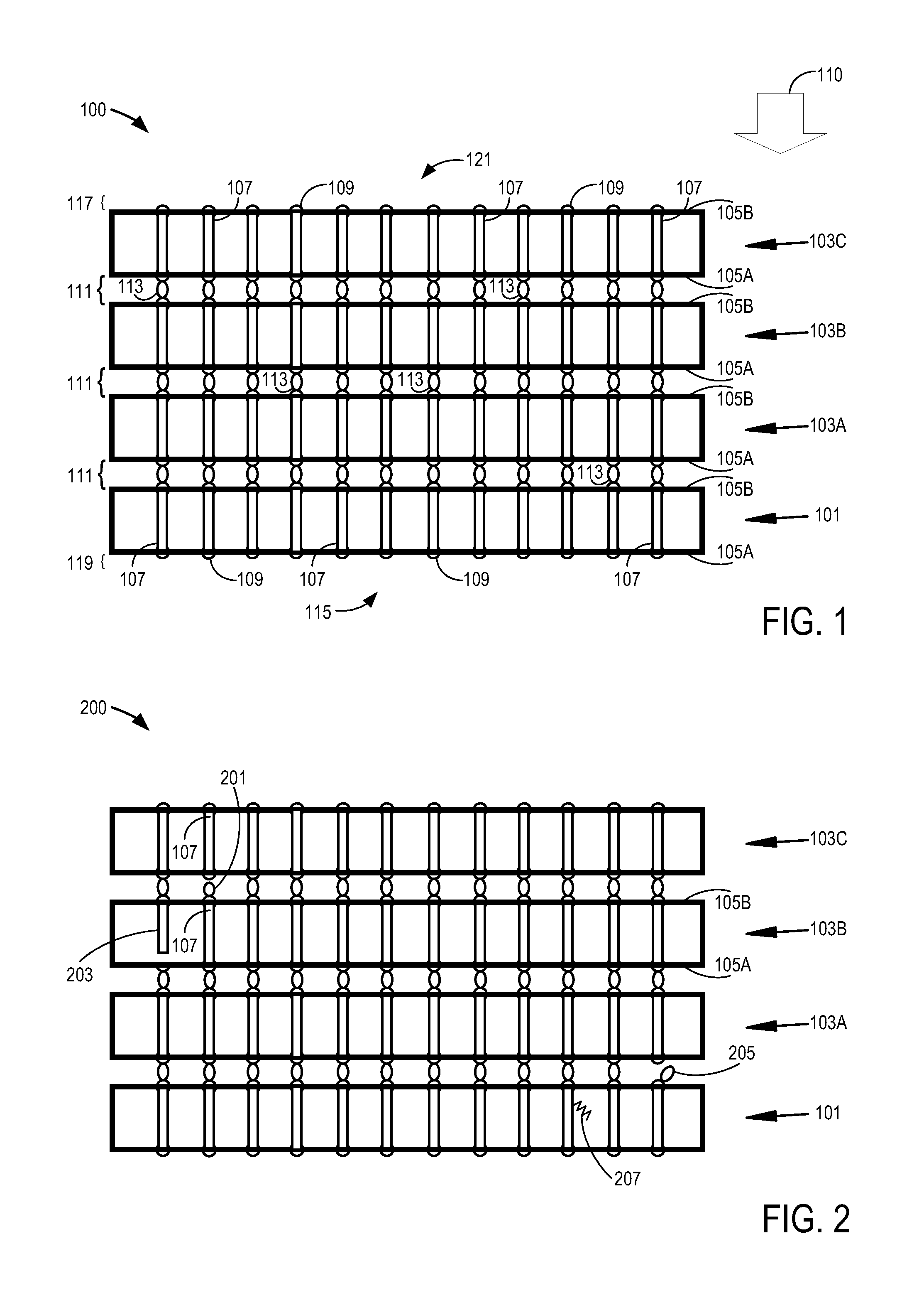
The shorted TSV 207 may cause drive and leakage issues depending upon a resistance value of the short and the short-tolerance or design of the connected electrical device.
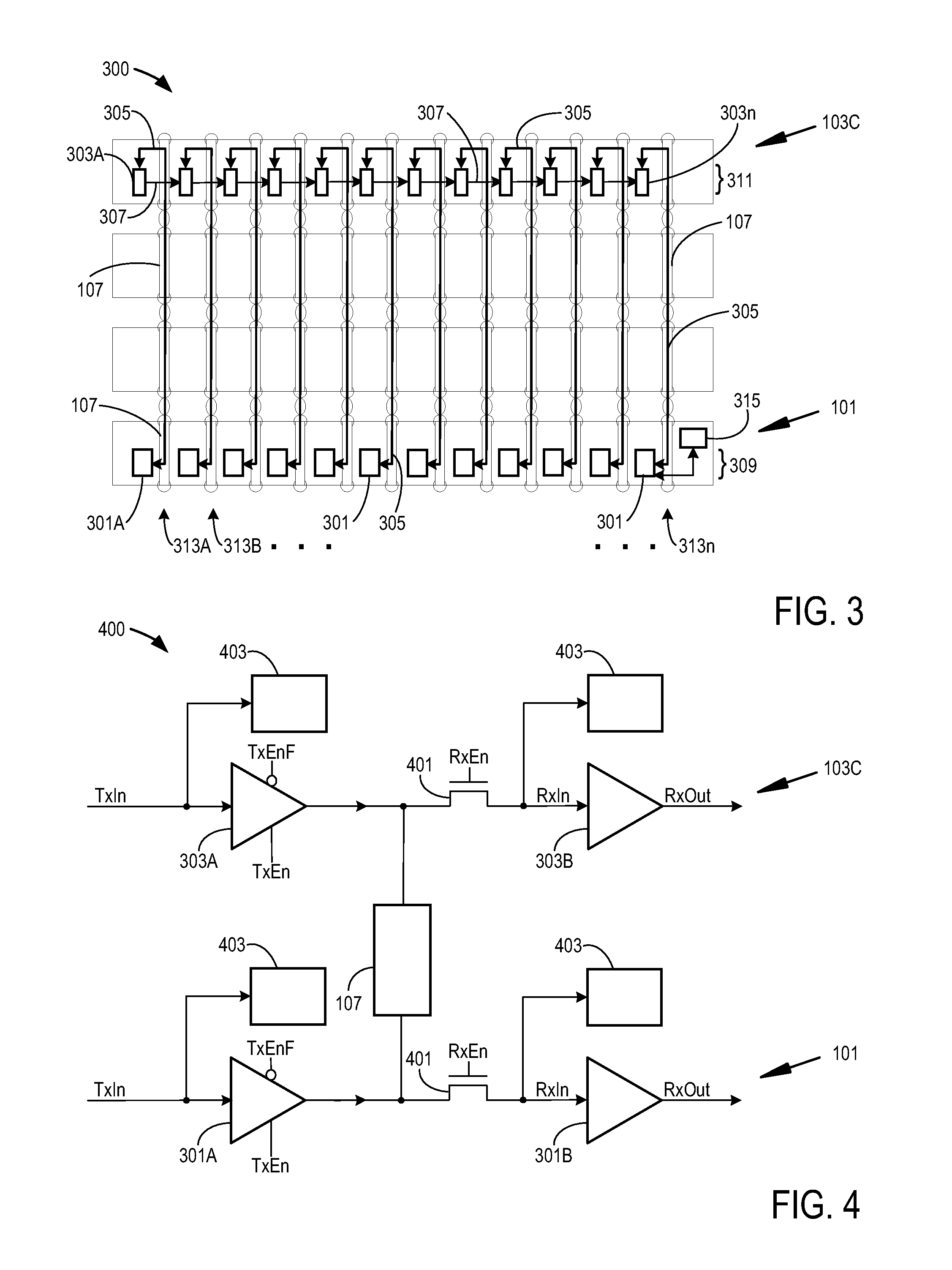
However, the portion of the transmitter / receiver circuit 400 may have a high failure probability if there are any defects with the TSV 107 as discussed above with regard to FIG. 2.
However, the redundant TSV 501 may not eliminate a TSV failure due to a short between either the TSV 107 or the redundant TSV 501 to the substrate.
However, in this case, since TSV 7 was found to be defective, the scan chain methodology was executed a second time and detected one the redundant TSVs 805 was also defective.

Method used


Image

  • Through-substrate via (TSV) testing
  • Through-substrate via (TSV) testing
  • Through-substrate via (TSV) testing

Examples


Embodiment Construction

[0013]In order to increase integrated circuit device density within a given area (e.g., a footprint on an electrical device or board), integrated circuit dice are often stacked on top of one another. One such example may be memory cards where a number of dice are stacked to increase an overall amount of memory. Each die has a number of integrated circuit devices fabricated on a substrate. However, each die within the stack frequently needs to communicate with other dice in the stack (e.g., slave dice typically need to communicate with a master die to perform their functions). Such stacks may be interconnected from one side of the substrate to the other. The interconnections include through-substrate vias (TSVs). When the substrate comprises silicon, the interconnections may also be referred to as through-silicon vias. If the TSVs are defective (e.g., are open or shorted), electrical communications may not occur throughout the stack as intended.

[0014]Referring now to FIG. 1, a cross-...


PUM


Abstract

Various embodiments comprise apparatuses and methods for testing and repairing through-substrate vias in a stack of interconnected dice. In various embodiments, an apparatus is provided that includes a number of through-substrate vias to couple to one or more devices, at least one redundant through-substrate via to allow a repair of the apparatus, and a pair of pull-up devices coupled to the through-substrate vias and the redundant through-substrate via to provide a high-data value to the first end of the respective through-substrate vias. A test register is coupled the second end of each of the through-substrate vias and the redundant through-substrate via to store a received version of the high-data value. A comparator compares the high-data value with the received version of the high-data value to test the through-substrate vias for short-circuit connections.

Description

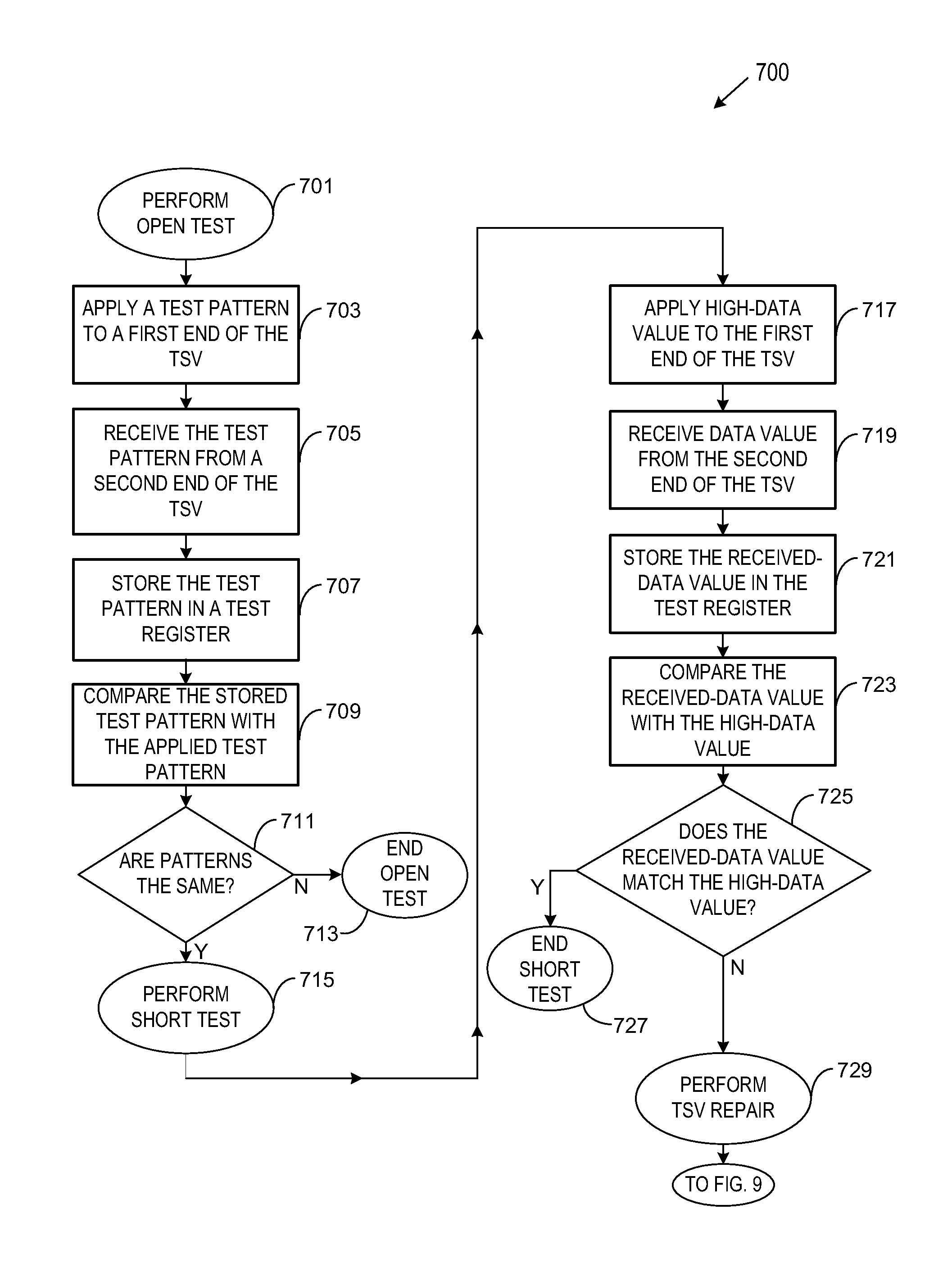
BACKGROUND[0001]Computers and other electronic systems, for example, digital televisions, digital cameras, and cellular phones, often have one or more memory devices to store information. Increasingly, memory or other devices are being reduced in size or have devices stacked to achieve a higher density of storage capacity within a similar footprint. However, stacked devices must still be robust in die-to-die communications.BRIEF DESCRIPTION OF THE DRAWINGS[0002]FIG. 1 shows a cross-sectional view of a microelectronics package having a number of stacked and interconnected integrated circuit dice;[0003]FIG. 2 shows a cross-sectional view of a microelectronics package having a number of stacked and interconnected integrated circuit dice with interconnect defects;[0004]FIG. 3 shows an illustrative embodiment for TSV testing using a scan chain arrangement;[0005]FIG. 4 shows an embodiment of a portion of a transmitter / receiver circuit used for TSV testing in the scan chain of FIG. 3;[0006...

Claims


Application Information

Patent Timeline
Patent Type & Authority Patents(United States)
IPC IPC(8): G01R31/3185H01L21/66G01R31/317
CPCG01R31/318513H01L22/22G01R31/31717H01L2924/0002H01L2924/00H01L23/481
Inventor BRINGIVIJAYARAGHAVAN, VENKATRAGHAVANBROWN, JASON M.
Owner MICRON TECH INC
Why Eureka
Eureka Blog
Learn More