Process for manufacturing a membrane microelectromechanical device, and membrane microelectromechanical device

a technology of microelectromechanical devices and manufacturing processes, applied in the direction of microstructural technology, decorative arts, chemical vapor deposition coatings, etc., can solve the problems of substrate etching, known processes suffer from certain limitations, and the manufacture of membrane microelectromechanical devices is, however, rather problemati

Inactive Publication Date: 2015-10-20
STMICROELECTRONICS SRL
View PDF20 Cites 2 Cited by
  • Summary
  • Abstract
  • Description
  • Claims
  • Application Information

AI Technical Summary

Problems solved by technology

The manufacture of membrane microelectromechanical devices is, however, rather problematical and, notwithstanding their wide diffusion, known processes suffer from certain limitations.
Substrate etch is, however, critical, both from the standpoint of costs and because the large thickness of the substrate (several hundreds of microns) poses problems of alignment and of feasibility of the etch.
In addition, the device obtained does not include any stopper structure capable of limiting the extension of the membrane towards the side of the substrate.
The membrane is hence not protected and may undergo failure.
The quality of the devices that can be obtained with the process described, however, is not optimal.
In fact, the membranes thus obtained present discontinuities that can give rise to structural defects or cracks, both during machining and in use, as a result of the stresses.
The relative brittleness of the membranes moreover requires rather large minimum thicknesses.
Solutions of this type are, however, very difficult to control, especially with regards to a crucial parameter as the final thickness of the membrane, and in any case are rather complex.

Method used


Image

  • Process for manufacturing a membrane microelectromechanical device, and membrane microelectromechanical device
  • Process for manufacturing a membrane microelectromechanical device, and membrane microelectromechanical device
  • Process for manufacturing a membrane microelectromechanical device, and membrane microelectromechanical device

Examples


Embodiment Construction

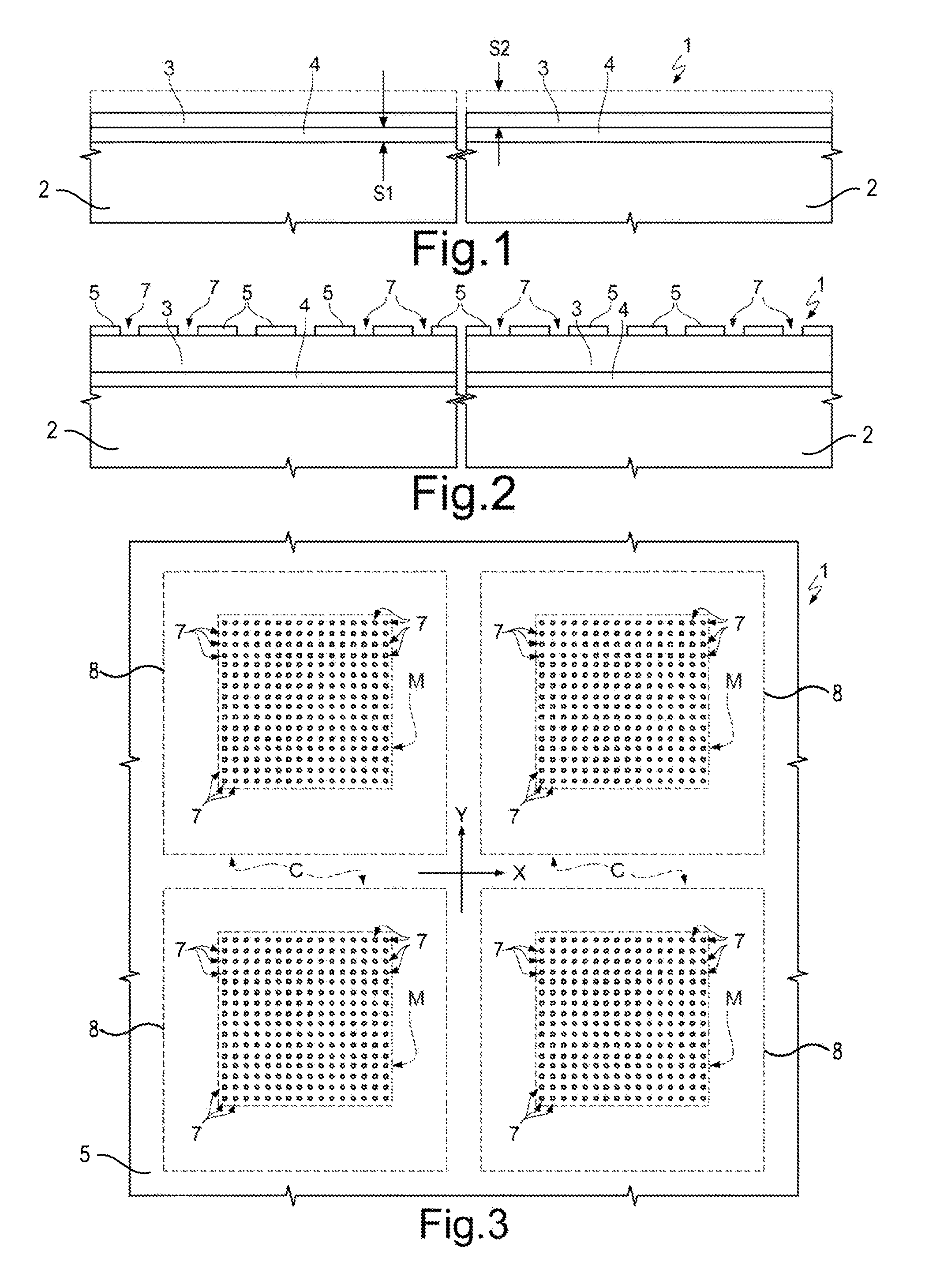
[0024]With reference to FIG. 1, a semiconductor wafer of a SOI type is designated as a whole by 1 and comprises a substrate 2, made of monocrystalline silicon, a structural layer 3, which is also made of monocrystalline silicon, and a dielectric layer 4, arranged between the substrate 2 and the structural layer 3. In one embodiment, the thickness 51 of the dielectric layer 4 is 1 μm.

[0025]By epitaxial growth, the structural layer 3 is extended as far as a desired thickness S2, for example of between 1 μm and 5 μm. In the embodiment described and illustrated herein, the thickness S2 of the structural layer 3 after the epitaxial growth is 2.5 μm.

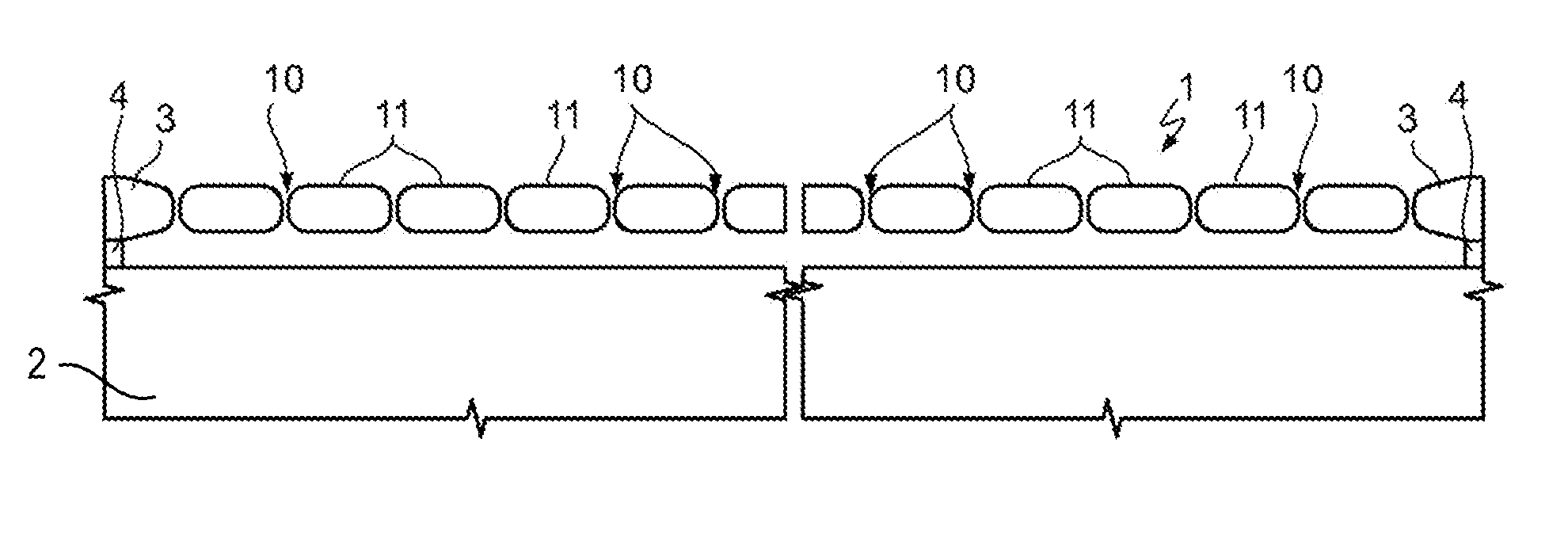
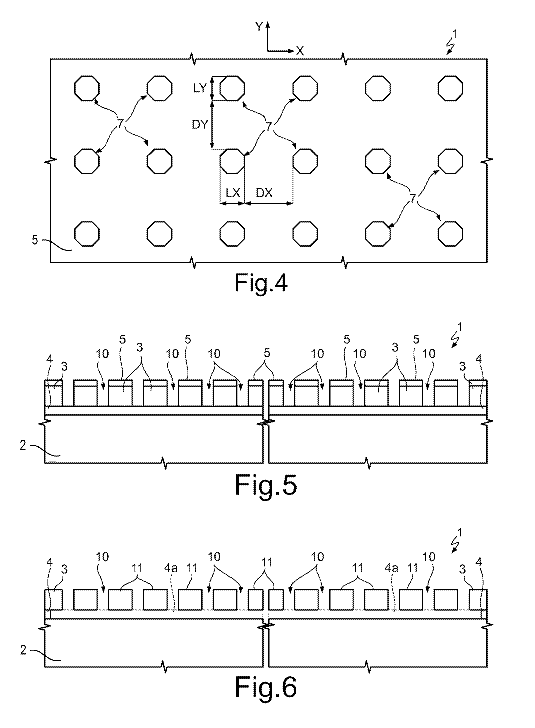
[0026]As shown in FIGS. 2-4, a mask 5 is formed on the structural layer 3. The mask 5 has apertures 7 arranged in an array in rows and columns along a first direction X and a second direction Y, respectively.

[0027]The apertures 7 are uniformly distributed in regions M intended for membranes, as may be seen in particular in FIG. 3, which shows ...


PUM

PropertyMeasurementUnit
temperatureaaaaaaaaaa
thicknessaaaaaaaaaa

Abstract

Disclosed herein is a microelectromechanical device and a process for manufacturing same. One or more embodiments may include forming a semiconductor structural layer separated from a substrate by a dielectric layer, and opening a plurality of trenches through the structural layer exposing a portion of the dielectric layer. A sacrificial portion of the dielectric layer is selectively removed through the plurality of trenches in membrane regions so as to free a corresponding portion of the structural layer to form a membrane. To close the trenches, the wafer is brought to an annealing temperature for a time interval in such a way as to cause migration of the atoms of the membrane so as to reach a minimum energy configuration.

Description

BACKGROUND[0001]1. Technical Field[0002]The present disclosure relates to a process for manufacturing a membrane microelectromechanical device and to a membrane microelectromechanical device.[0003]2. Description of the Related Art[0004]As is known, semiconductor-machining techniques have made it possible to provide membrane microelectromechanical devices that may be used as sensors or transducers in various applications. For example, known to the art are capacitive pressure sensors, in which a semiconductor membrane separates a reference pressure chamber from the external environment. The difference between the external pressure and the reference pressure modifies the configuration of the membrane and hence the capacitive coupling between the membrane itself and the opposite wall of the chamber. In other cases, the deformation of the membrane is detected by exploiting the piezoresistive properties of monocrystalline silicon. Microelectromechanical membrane transducers are frequently...

Claims


Application Information

Patent Timeline
Patent Type & Authority Patents(United States)
IPC IPC(8): B81C1/00G01L9/00
CPCB81C1/00158B81C1/00293G01L9/0042G01L9/0073B81B2201/0257B81B2203/0127B81C2203/0145B81C2201/0116
Inventor CORONA, PIETROFERRERA, MARCOVARISCO, IGORCAMPEDELLI, ROBERTO
Owner STMICROELECTRONICS SRL
Why Eureka
Try Eureka