Making electrical components in handle wafers of integrated circuit packages

Active Publication Date: 2015-10-20
INVENSAS CORP
View PDF101 Cites 220 Cited by
  • Summary
  • Abstract
  • Description
  • Claims
  • Application Information

AI Technical Summary

Benefits of technology

[0010]In accordance with embodiments of the present invention, methods are provided for fabricating discrete electrical components, viz., capacitors, within a first substrate, e.g., a handle wafer, of an integrated circuit (IC) package, which also contains cavities for housing integrated circuit

Problems solved by technology

However, a practical problem arises when the interposer wafer of such packages is made substantially thin, in that this limits the vertical height of the discrete electrical components, such as capacitors, that can be built into the

Method used


Image

  • Making electrical components in handle wafers of integrated circuit packages
  • Making electrical components in handle wafers of integrated circuit packages
  • Making electrical components in handle wafers of integrated circuit packages

Examples


Example

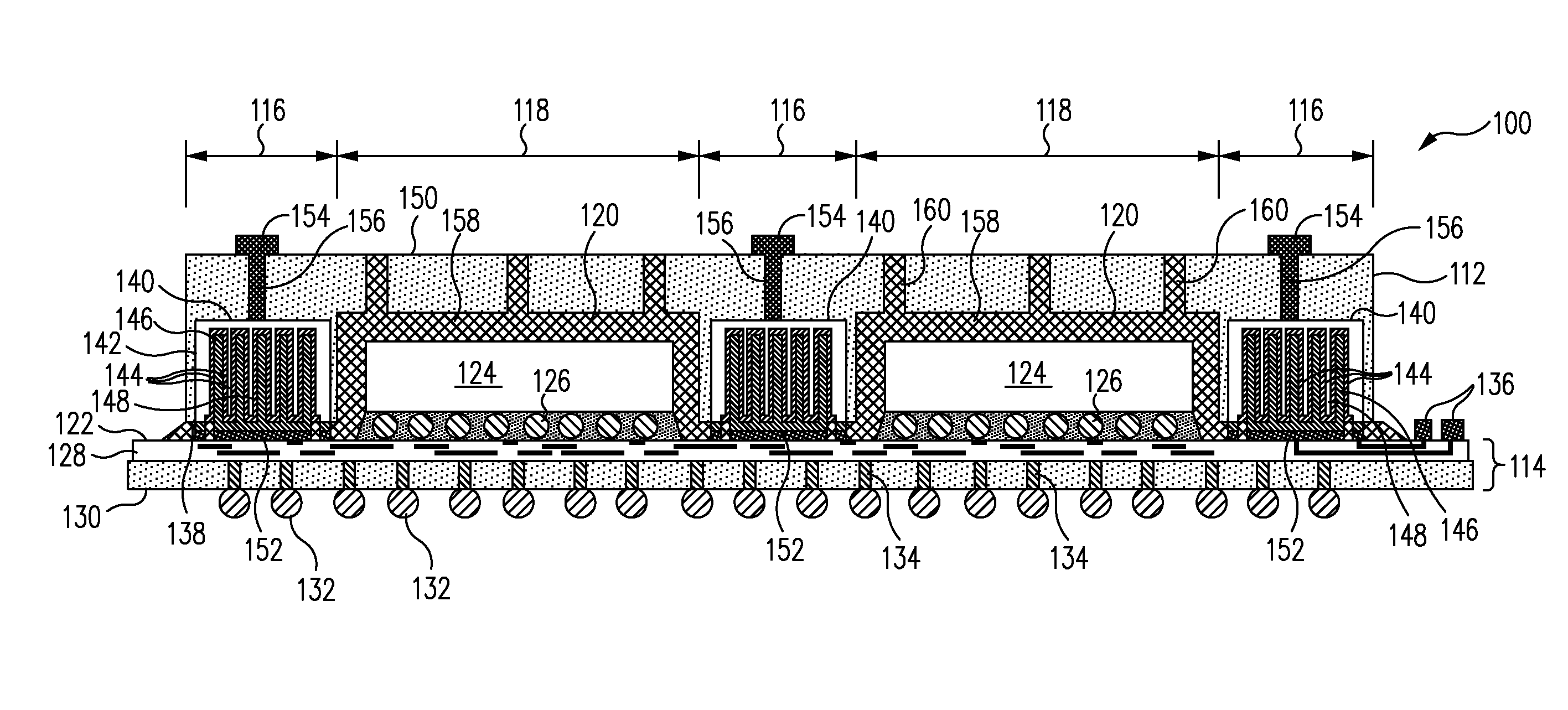
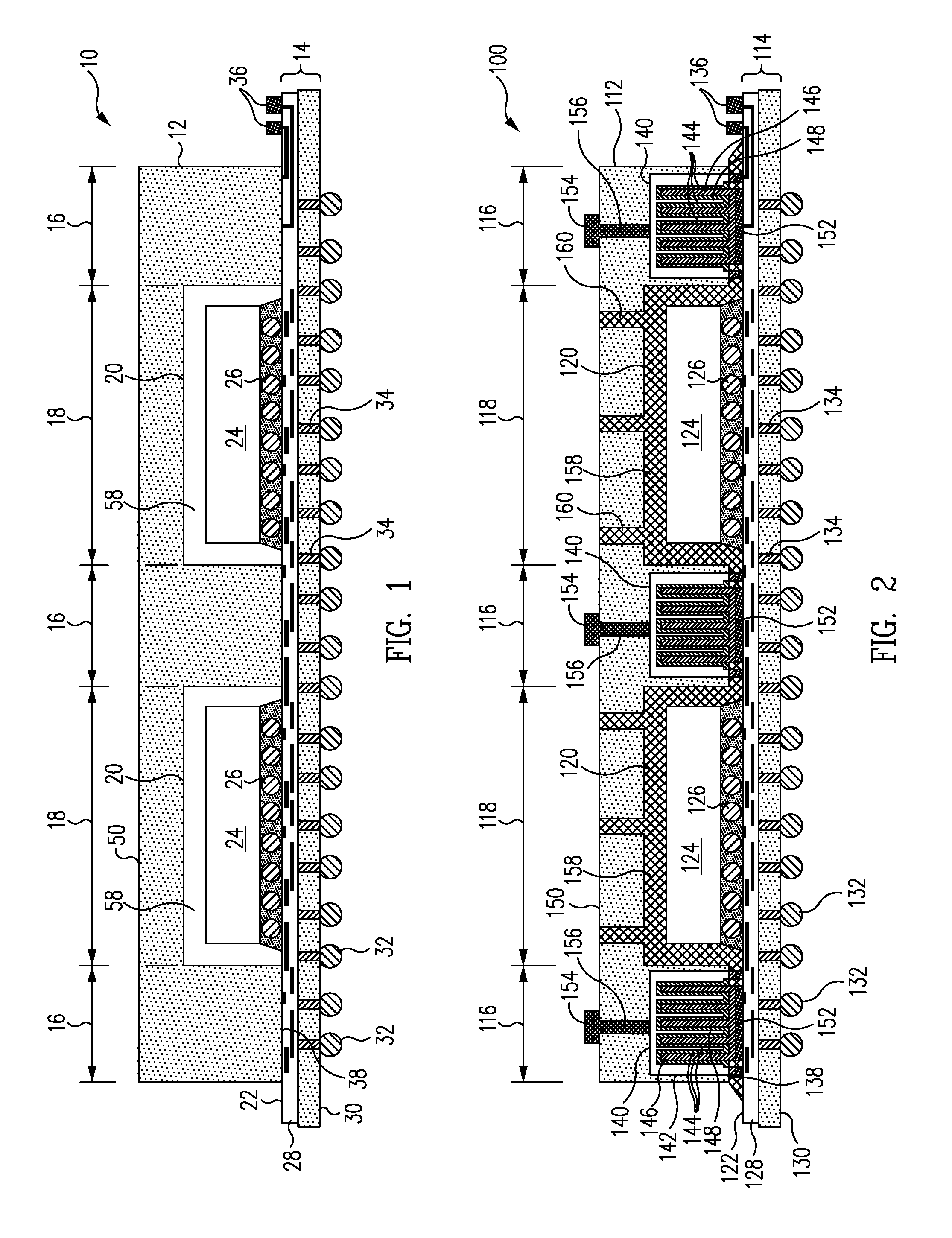
[0019]This disclosure provides embodiments of methods for making semiconductor packages in which electrical components, viz., metal-insulator-metal (MIM) capacitors, are fabricated within selected regions of a first substrate, such as a handle wafer, that contains cavities for housing integrated circuit dies or packages mounted on a second, associated substrate, e.g., an interposer wafer. The methods result in a more efficient use of package volume, and hence, semiconductor packages of a reduced size and / or enhanced functionality.

[0020]FIG. 1 is a vertical cross-sectional view of an example embodiment of an IC package 10 of a type disclosed in commonly owned U.S. patent application Ser. No. 14 / 214,365 above, and to which the methods and apparatus of the present invention can be advantageously applied. As discussed above, the package 10 comprises a “sandwich” of a first substrate, or “handle wafer”12, and a second substrate, or “interposer”14. The handle wafer 12 includes at least on...


PUM


Abstract

A method for making an integrated circuit package includes providing a handle wafer having a first region defining a cavity. A capacitor is formed in the first region. The capacitor has a pair of electrodes, each coupled to one of a pair of conductive pads, at least one of which is disposed on a lower surface of the handle wafer. An interposer having an upper surface with a conductive pad and at least one semiconductor die disposed thereon is also provided. The die has an integrated circuit that is electroconductively coupled to a redistribution layer (RDL) of the interposer. The lower surface of the handle wafer is bonded to the upper surface of the interposer such that the die is disposed below or within the cavity and the electroconductive pad of the handle wafer is bonded to the electroconductive pad of the interposer in a metal-to-metal bond.

Description

BACKGROUND[0001]1. Technical Field[0002]This disclosure generally relates to making integrated circuit packages with “handle wafers,” and more particularly, to making discrete electrical components, such as capacitors, within the handle wafers of such packages.[0003]2. Related Art[0004]The “wafer level” or “wafer scale” production of integrated circuit (IC) packages has proliferated in recent years, due primarily to the economies of scale that such production techniques afford, together with the concomitant reduction in size and cost of the resulting packages.[0005]Examples of such IC packages and methods for making them can be found in, e.g., commonly owned U.S. patent application Ser. No. 14 / 214,365 by H. Shen, et al., filed Mar. 14, 2014, and entitled “Integrated Circuits Protected by Substrates with Cavities, and Methods of Manufacture,” the entire disclosure of which is incorporated herein by reference.[0006]In one of only many possible embodiments of such packages, the package...

Claims


Application Information

Patent Timeline
IPC IPC(8): H01L21/00H01L21/56
CPCH01L21/56H01L25/105H01L25/11H01L25/115H01L25/50H01L2224/16225H01L2224/32225H01L2224/73204H01L2924/15311H01L2924/16153H01L25/165H01L28/40H01L28/60H01L28/65H01L2924/00H01L21/4853H01L21/486H01L23/49827H01L23/49833H01L23/49838H01L24/05H01L24/83H01L2224/05009H01L2924/1205H01L23/5223H01L24/32
Inventor WANG, LIANGSHEN, HONGKATKAR, RAJESH
Owner INVENSAS CORP
Why Eureka
Try Eureka