Laser devices using a semipolar plane

a laser device and semi-polar plane technology, applied in the field of optical devices, can solve the problems of 0.1% efficiency of wall plugs, 80% power consumption, routine failure, etc., and achieve the effect of reducing the degradation of quantum wells or light emitting regions, low resistance p-cladding, and good device performan

Active Publication Date: 2015-10-20
KYOCERA SLD LASER INC
View PDF215 Cites 9 Cited by
  • Summary
  • Abstract
  • Description
  • Claims
  • Application Information

AI Technical Summary

Benefits of technology

[0013]We expect that this material on (20-2-1) with narrow FWHM and red-shifting wavelength translates into higher gain laser diodes, which will allow us to further improve the wall plug efficiency in both the blue and green wavelength regimes. In the blue regime, this could be important for high power laser diode where we would apply a very low reflectivity (1-7%) coating to the front facet for high slope efficiency, but still maintain low threshold current with the high material gain.
[0019]5. We believe that by using (20-2-1) in green laser diode we will be able to increase the gain and hence increase the wall plug efficiency to greater than about 5%, greater than about 7%, or greater than about 10%.
[0020]In other embodiments, the present device uses an InGaN / GaN superlattice structure below the active region to improve the material quality of the active region causing the electroluminescence to be brighter. In a specific embodiment the super lattice also functions as a separate confinement heterostructure (SCH) in a laser diode. This superlattice is required for good epi quality, but will also help guide the optical mode for increased optical confinement within the gain-providing quantum well layers. In a specific embodiment, the superlattice is part of the waveguide. In a specific embodiment, the present method and device may be configured with the following.
[0031]The method and device here can be configured with conductive oxides, low temperature p-clad, n-contact scribes, beam clean-up scribes, among others. It can also include an indium tin oxide (ITO) or zinc oxide (ZnO) cladding region on top of a thin p-type layer such as p-GaN layer or region of 200 Å to 2000 Å for laser diodes or LEDs. Certain GaN planes may suffer from severe thermal degradation in the active region during growth of the electron blocking layer and the p-cladding layers where elevated temperatures are used. In certain embodiments, if ZnO or ITO is formed in place of a portion or substantially the p-clad layer or region, desirable p-type material can be achieved without subjecting the resulting device to a long growth time of the p-layer.
[0032]In a specific embodiment, the method and device can also include growth of a very low temperature p-cladding on top of the quantum well or light emitting layers. By developing epitaxial conditions that enable low resistance p-cladding sufficient for good device performance with a growth temperature of 700° C. to 800° C., 800° C. to 850° C., or 850° C. to 875° C. degradation to the quantum well or light emitting regions can be reduced.
[0033]The invention enables a cost-effective optical device for laser applications such as display technologies. The optical device can be manufactured in a relatively simple and cost effective manner. The laser device uses a semipolar gallium nitride material capable of achieve a green laser device. The laser device is capable of emitting long wavelengths such as those ranging from about 480 nm to about 540 nm, and also from about 540 nm to about 660 nm. In alternative embodiments, the laser device is capable of emitting blue wavelengths, e.g., those ranging from about 420 nm to about 480 nm.

Problems solved by technology

Unfortunately the Edison light bulb dissipates most of the power consumed as thermal energy.
It routinely fails due to thermal expansion and contraction of the filament element.
The Ar-ion laser had the benefit of producing highly directional and focusable light with a narrow spectral output, but the wall plug efficiency was <0.1%, and the size, weight, and cost of the lasers were undesirable as well.
As laser technology evolved, more efficient lamp pumped solid state laser designs were developed for the red and infrared wavelengths, but these technologies remained a challenge for blue and green and blue lasers.
The resulting green and blue lasers were called “lamped pumped solid state lasers with second harmonic generation” (LPSS with SHG) had wall plug efficiency of −1%, and were more efficient than Ar-ion gas lasers, but were still too inefficient, large, expensive, fragile for broad deployment outside of specialty scientific and medical applications.
Additionally, the gain crystal used in the solid state lasers typically had energy storage properties which made the lasers difficult to modulate at high speeds which limited its broader deployment.
However, the change to diode pumping increased the system cost and required precise temperature controls, leaving the laser with substantial size, power consumption while not addressing the energy storage properties which made the lasers difficult to modulate at high speeds.
These lasers designs are meant to improve the efficiency, cost and size compared to DPSS-SHG lasers, but the specialty diodes and crystals required make this challenging today.
Additionally, while the diode-SHG lasers have the benefit of being directly modulate-able, they suffer from severe sensitivity to temperature which limits their application.

Method used


Image

  • Laser devices using a semipolar plane
  • Laser devices using a semipolar plane
  • Laser devices using a semipolar plane

Examples


Embodiment Construction

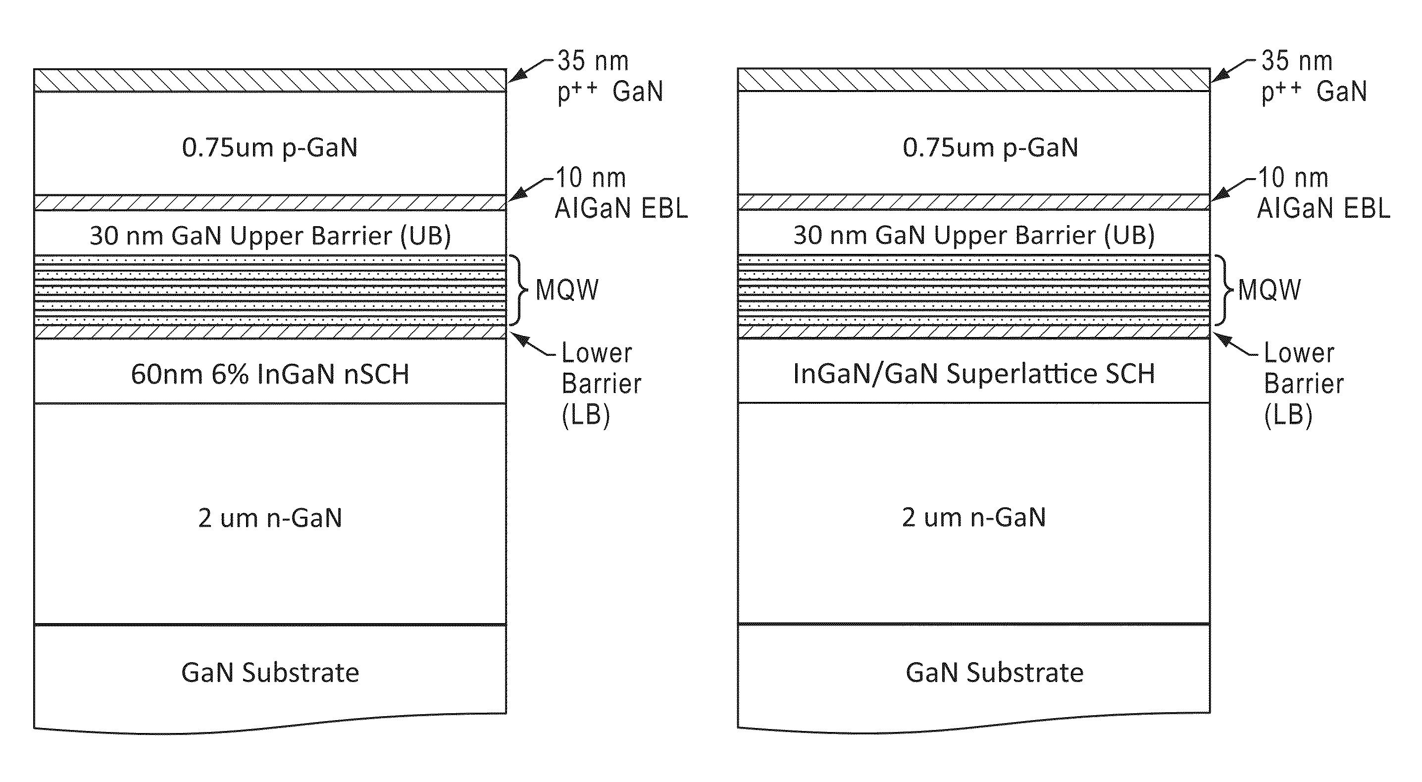
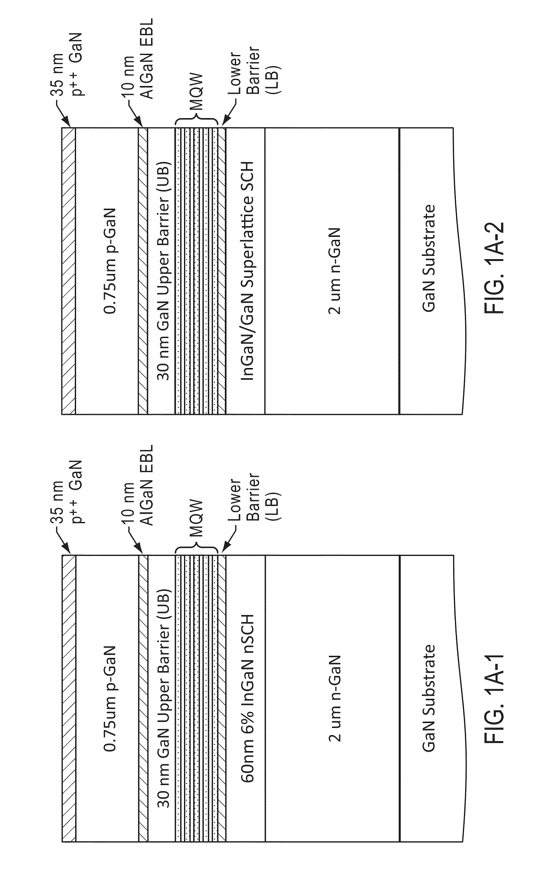
[0053]FIGS. 1A-1, 1A-2, 1B-1, and 1B-2 are diagrams of optical devices including growth regions according to an embodiment of the present invention. As shown, the laser diode is an epitaxial structure configured on a gallium and nitrogen containing substrate within a family of planes, e.g., (30-3-2), (20-2-1), (30-3-1), (30-32), (20-21), (30-31) or any orientation within + / −10 degrees toward c-plane and / or a-plane from these orientations. In a specific embodiment referring to FIG. 1A-1, the gallium nitride substrate includes an n-type gallium and nitride epitaxial region, an overlying InGaN nSCH region, a lower barrier region, a plurality of quantum well regions, an upper barrier region, an electron blocking region, a p-type gallium and nitrogen containing region, and an overlying p++ GaN contact region. Referring now to FIG. 1A-2, the gallium nitride substrate includes an n-type gallium and nitride epitaxial region, an overlying InGaN / GaN superlattice SCH region, a lower barrier re...


PUM


Abstract

An optical device includes a gallium and nitrogen containing substrate comprising a surface region configured in a (20-2-1) orientation, a (30-3-1) orientation, or a (30-31) orientation, within + / −10 degrees toward c-plane and / or a-plane from the orientation. Optical devices having quantum well regions overly the surface region are also disclosed.

Description

[0001]This application is a continuation of U.S. application Ser. No. 13 / 651,291, filed Oct. 12, 2012, which claims the benefit of U.S. Provisional Application No. 61 / 546,792 filed on Oct. 13, 2011, both of which are incorporated by reference herein in their entirety.BACKGROUND[0002]The present invention is directed to optical devices and related methods. In particular, the invention provides a method and device for emitting electromagnetic radiation using nonpolar or semipolar gallium containing substrates such as GaN, AlN, InN, InGaN, AlGaN, and AlInGaN, and others. More particularly, the present invention provides a method and device using a gallium and nitrogen containing substrate configured on the {20-21} family of planes or an off-cut of the {20-21} family of planes toward the plus or minus c-plane and / or toward the a-plane according to one or more embodiments, but there can be other configurations. Such family of planes include, but are not limited to, (30-3-2), (20-2-1), (3...

Claims


Application Information

Patent Timeline
Patent Type & Authority Patents(United States)
IPC IPC(8): H01S5/00H01S5/34H01S5/343
CPCH01S5/34333H01S5/3401H01S5/0014H01S5/22H01S5/3216H01S5/3214H01L33/08H01L33/16H01S5/2009H01S5/320275H01S5/2031H01S5/04252H01S2301/176H10N30/082H01S5/2201H01L21/0274H01L21/042H01L21/28123H01L21/302H01L21/311H01L21/461H01L21/469H01L21/4828H01S5/028H01S5/0287H01S5/2214
Inventor RARING, JAMES W.LIN, YOU-DAELSASS, CHRISTIANE
Owner KYOCERA SLD LASER INC
Why Eureka
Try Eureka