

Circuits and methods of a self-timed high speed SRAM
a high-speed sram and circuit technology, applied in the direction of information storage, static storage, digital storage, etc., can solve the problems of short propagation delay, inability to generate control signals, waste of excess power, etc., to save power, enhance the driving capability of the reference cell, and save the same device size, area, shape and structure
- Summary
- Abstract
- Description
- Claims
- Application Information
AI Technical Summary
Benefits of technology
Problems solved by technology
Method used
Image

Examples
Embodiment Construction
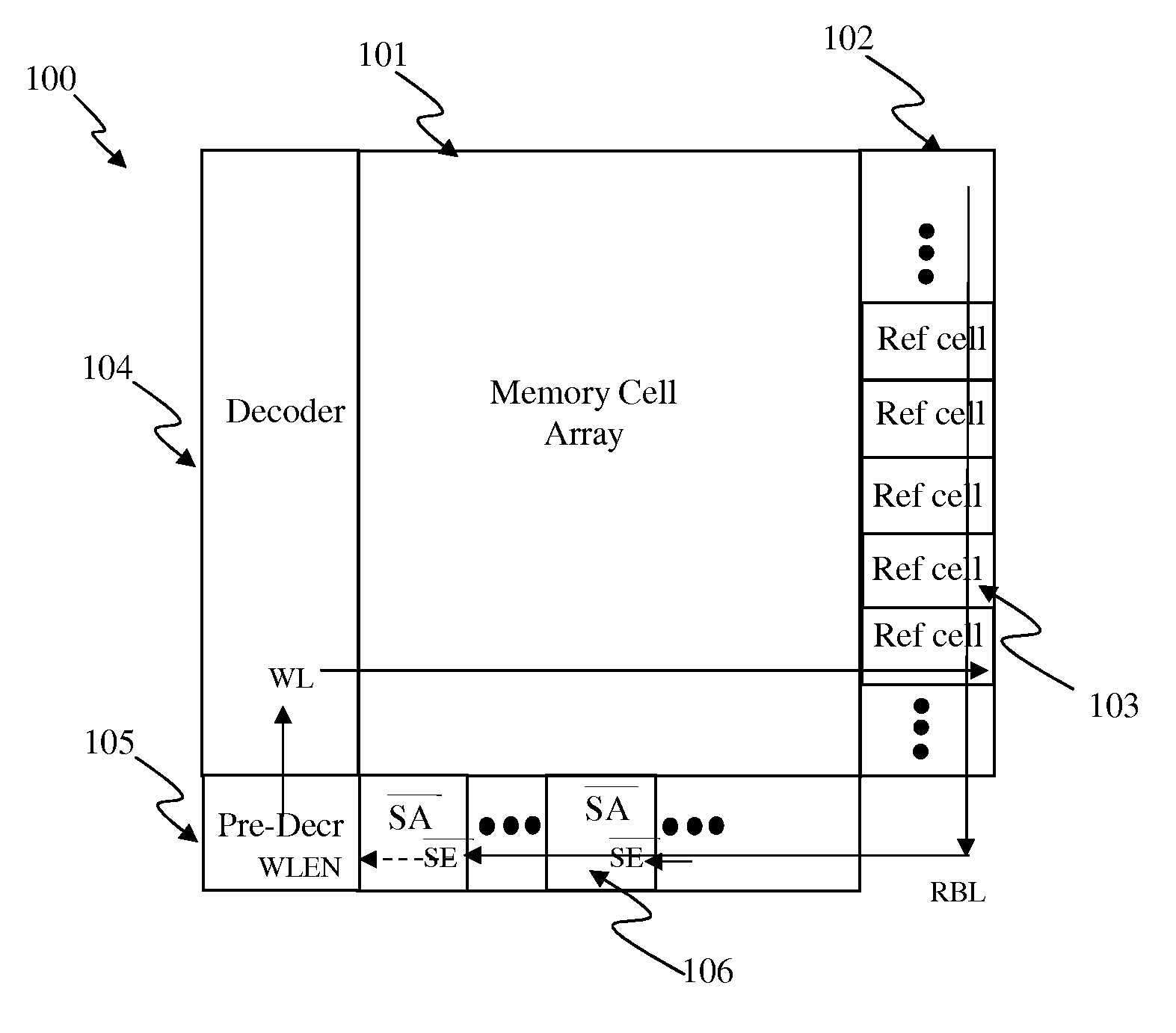
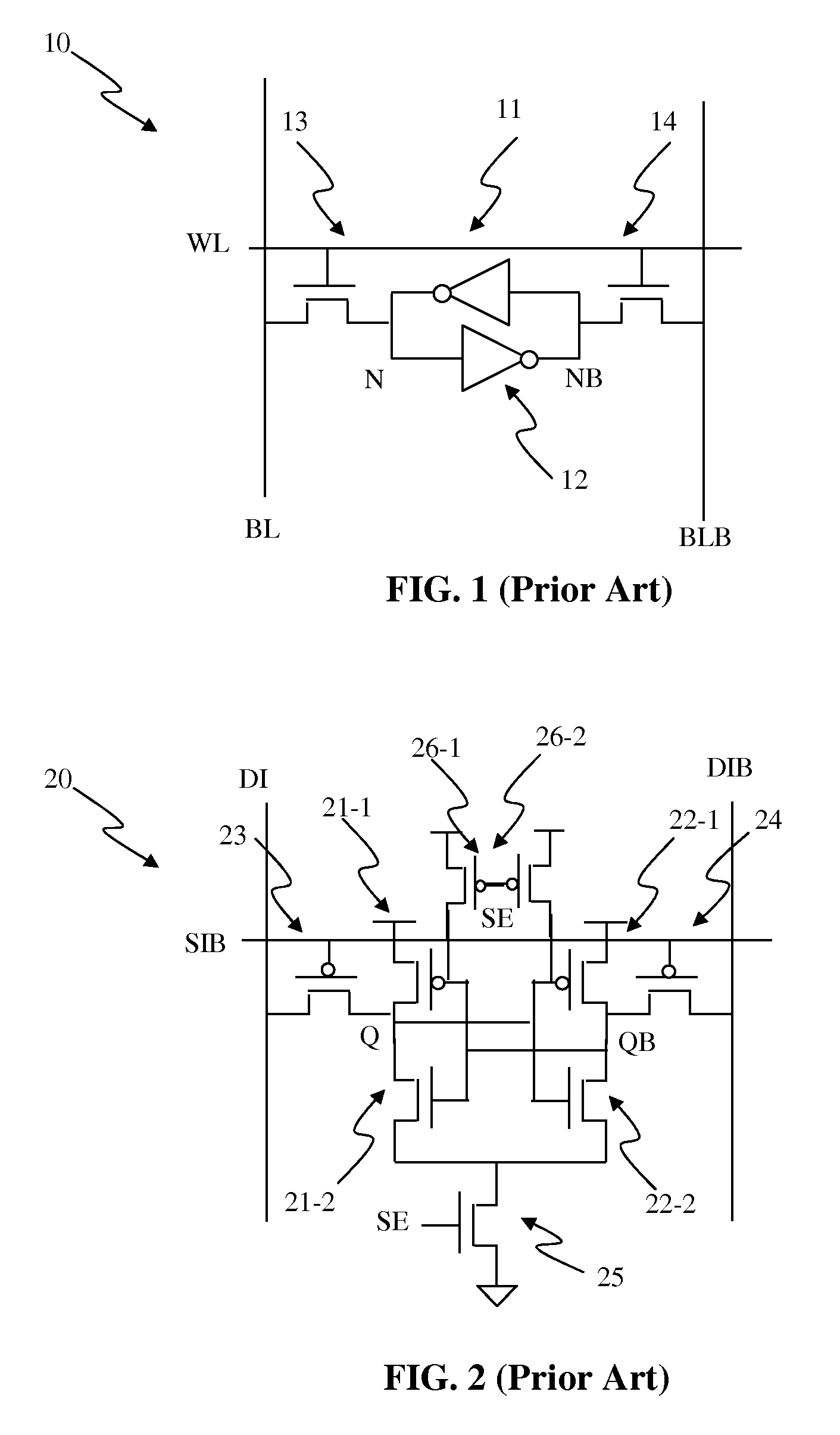
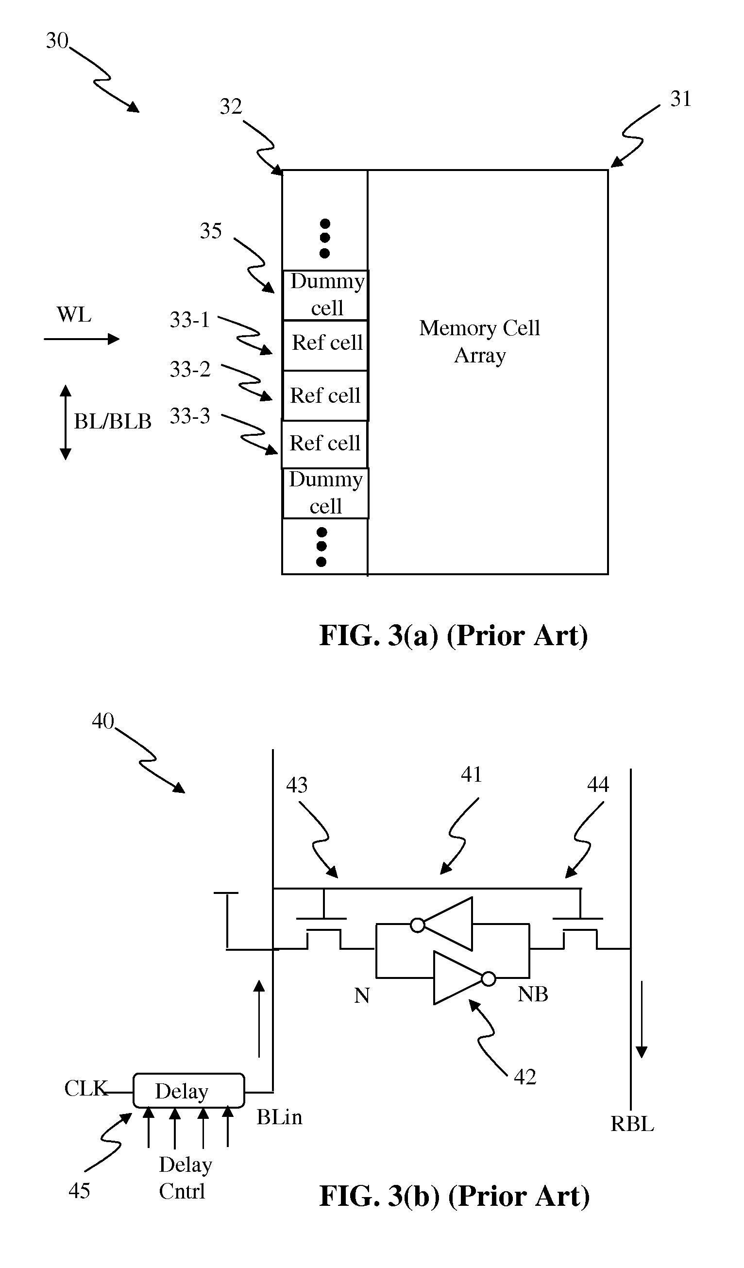
[0038]Embodiments disclosed herein can track wordline and / or bitline delays to activate at least one sense amplifier (SA) and to turn off a wordline after at least one sense amplifier (SA) is activated. A latch-type of SA is essential in today's nanometer SRAM for low power and low voltage operations. However, the latch-type of SA requires sufficient signal splits developed in the input of an SA before being activated; otherwise irrevocable incorrect data can be sensed and latched. Without sufficient timing margins, the input signals may not be split wide enough for sensing. On the other hand, if the timing margins are too wide, the speed of an SRAM can suffer. Advantageously, embodiments disclosed herein are capably of tracking critical timings to achieve reliable operations and yet high speed by using at least one reference cell, similar to the normal cell, to track wordline and / or bitline delay and to turn on at least one sense amplifier accordingly. After the SA is activated, th...
PUM
 Abstract
Description
Claims
Application Information