Unlock instant, AI-driven research and patent intelligence for your innovation.

Control method for nonvolatile memory device with vertically stacked structure

a nonvolatile memory and control method technology, applied in the field of nonvolatile memory devices, can solve problems such as errors

Active Publication Date: 2015-12-22
SOLID STATE STORAGE TECH CORP
View PDF7 Cites 1 Cited by
  • Summary
  • Abstract
  • Description
  • Claims
  • Application Information

AI Technical Summary

Benefits of technology

This approach significantly reduces data error rates in program and read modes by maintaining a stable voltage at the common source line, improving the operational accuracy of the nonvolatile memory device.

Problems solved by technology

The voltage drifting caused by the electrical resistance of the common source line CSL may induce erroneous actions of the conventional nonvolatile memory device with the vertically stacked structure in various operating modes.

Method used


Image

  • Control method for nonvolatile memory device with vertically stacked structure
  • Control method for nonvolatile memory device with vertically stacked structure
  • Control method for nonvolatile memory device with vertically stacked structure

Examples


Embodiment Construction

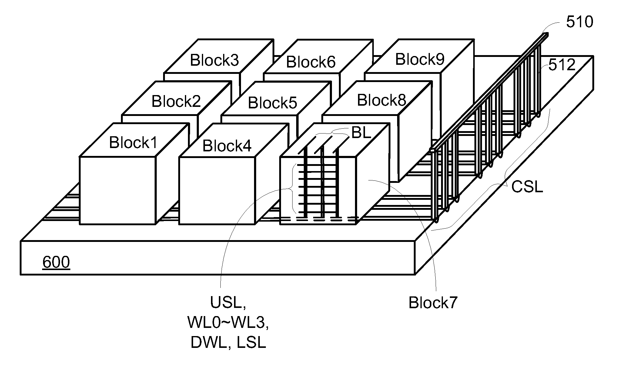
[0030]FIG. 4 schematically illustrates a nonvolatile memory device with a vertically stacked structure composed of plural memory blocks. As shown in FIG. 4, plural memory blocks are formed on a semiconductor substrate 400. Each memory block has the configurations as shown in FIG. 2. For example, as shown in FIG. 4, at least the x-th memory block Blockx and a y-th memory block Blocky are formed on the semiconductor substrate 400.

[0031]The x-th memory block Blockx comprises bit lines BL0x˜BL2x, an upper selection line USLx, a lower selection line LSLx, word lines WL0x˜WL3x, and a dummy word line DWLx.

[0032]Similarly, the y-th memory block Blocky comprises bit lines BL0y˜BL2y, an upper selection line USLy, a lower selection line LSLy, word lines WL0y˜WL3y, and a dummy word line DWLy.

[0033]The common source lines CSL between the x-th memory block Blockx and the y-th memory block Blocky are connected with each other through common source lines CSL. That is, the x-th memory block Blockx a...


PUM


Abstract

A control method for a nonvolatile memory device with a vertically stacked structure is provided. The nonvolatile memory device includes a substrate, a common source line formed on the substrate, and plural memory blocks disposed over the substrate. Each memory block includes a cell string connected between a bit line and the common source line. Firstly, a first memory block of the plural memory blocks is selected as an active memory block, and one of the remaining memory blocks is selected as a second memory block. Then, a ground voltage is provided to the bit line of the second memory block, and the cell string of the second memory block is conducted, so that the ground voltage is transmitted from the bit line to the common source line through the cell string.

Description

[0001]This application claims the benefit of People's Republic of China Application Serial No. 201310744294.4, filed Dec. 30, 2013, the subject matter of which is incorporated herein by reference.FIELD OF THE INVENTION[0002]The present invention relates to a nonvolatile memory device, and more particularly to a control method for a nonvolatile memory device with a vertically stacked structure.BACKGROUND OF THE INVENTION[0003]FIG. 1 is a schematic cross-sectional view illustrating a conventional nonvolatile memory device with a vertically stacked structure. For example, this nonvolatile memory device is disclosed in U.S. Pat. No. 8,278,170.[0004]A common source line CSL is formed on a semiconductor substrate 100. The common source line CSL is an N-type doping region of the semiconductor substrate 100. Lower interlayer dielectric layers 111˜114 and lower conduction patterns LSL, WL0 and WL1 are alternately stacked on the semiconductor substrate 100.[0005]Moreover, lower active pillars...

Claims


Application Information

Patent Timeline
Patent Type & Authority Patents(United States)
IPC IPC(8): G11C7/00G11C7/12G11C7/14G11C7/18G11C7/22G11C5/02
CPCG11C5/02G11C7/18G11C7/14G11C7/12G11C5/025G11C5/063G11C16/10
Inventor LIN, CHRONG-JUNGPAN, HSIN-WEI
Owner SOLID STATE STORAGE TECH CORP