Electro-optical device and electronic apparatus

a technology of optical devices and electronic devices, applied in semiconductor devices, identification means, instruments, etc., can solve the problems of inaccurate luminance, inability to increase the size of capacitors connected to gate nodes, uneven luminance, etc., and achieve the effect of reducing image quality degradation

Active Publication Date: 2015-12-29
SEIKO EPSON CORP
View PDF6 Cites 7 Cited by
  • Summary
  • Abstract
  • Description
  • Claims
  • Application Information

AI Technical Summary

Benefits of technology

[0007]An advantage of some aspects of the invention is that it reduces degradations in image quality associated with variations in the potential of data lines.
[0009]According to the aspects of the invention, among a plurality of relay electrodes that electrically connect gate electrodes of driving transistors to given nodes, a first relay electrode formed in the same layer as the data line is surrounded on at least three sides by the power supply wiring line. This reduces invasion of noise from the data line to a connection portion of the gate electrode of the driving transistor. As a result, variations in the potential of the gate electrode of the driving transistor are controlled, and the current supplied via the driving transistor to a light emitting element will not change. Thus, display with accurate luminance will be performed.
[0010]In the above electro-optical device, an initializing power supply wiring line or a power supply wiring line on a low side of a power supply may be used as the power supply wiring line. These power supply wiring lines are lower in impedance than a power supply wiring line used in the scanning line driving circuit, the data line driving circuit, or the like, their shield effects improve more.
[0011]In the above electro-optical device, it is preferable that the power supply wiring line is formed so as to be at a position between the first relay electrode and the data line, and the first relay electrode is surrounded by the power supply wiring line. Since the power supply wiring line surrounding the first relay electrode is at a position between the first relay electrode and the data line, the first relay electrode is shielded from noise radiated from the data line by the power supply wiring line. Thus, invasion of noise from the data line to the connection portion of the gate electrode of the driving transistor is suppressed. This enables display quality to be improved.
[0012]In the above electro-optical device, it is preferable that the first relay electrode is surrounded on four sides by an opening formed in the power supply wiring line. Since the first relay electrode is formed in the opening and is surrounded on four sides by the opening, its shield effect is improved more.
[0013]In the above electro-optical device, it is preferable that a second relay electrode formed in a different layer from the first relay electrode and electrically connecting the gate electrode of the driving transistor to the given node is provided, and the second relay electrode is surrounded on at least three sides by a power supply wiring line on a high side of a power supply formed in the same layer as the second relay electrode. According to the aspects of the invention, the second relay electrode is surrounded on three sides by the high-side power supply wiring line. A high shield effect is therefore attained.

Problems solved by technology

When a pixel circuit having a configuration as mentioned above is actually driven, variations in the potential levels of data lines cause noise.
Therefore, when the noise affects the gate node of the driving transistor, an accurate luminance cannot be displayed.
Thus, there is unevenness in luminance.
In particular, this becomes a large problem in the case where a storage capacitor connected to the gate node cannot be increased in size.
The variation is visually recognized as luminance unevenness, causing a decrease in display quality.

Method used


Image

  • Electro-optical device and electronic apparatus
  • Electro-optical device and electronic apparatus
  • Electro-optical device and electronic apparatus

Examples


embodiment

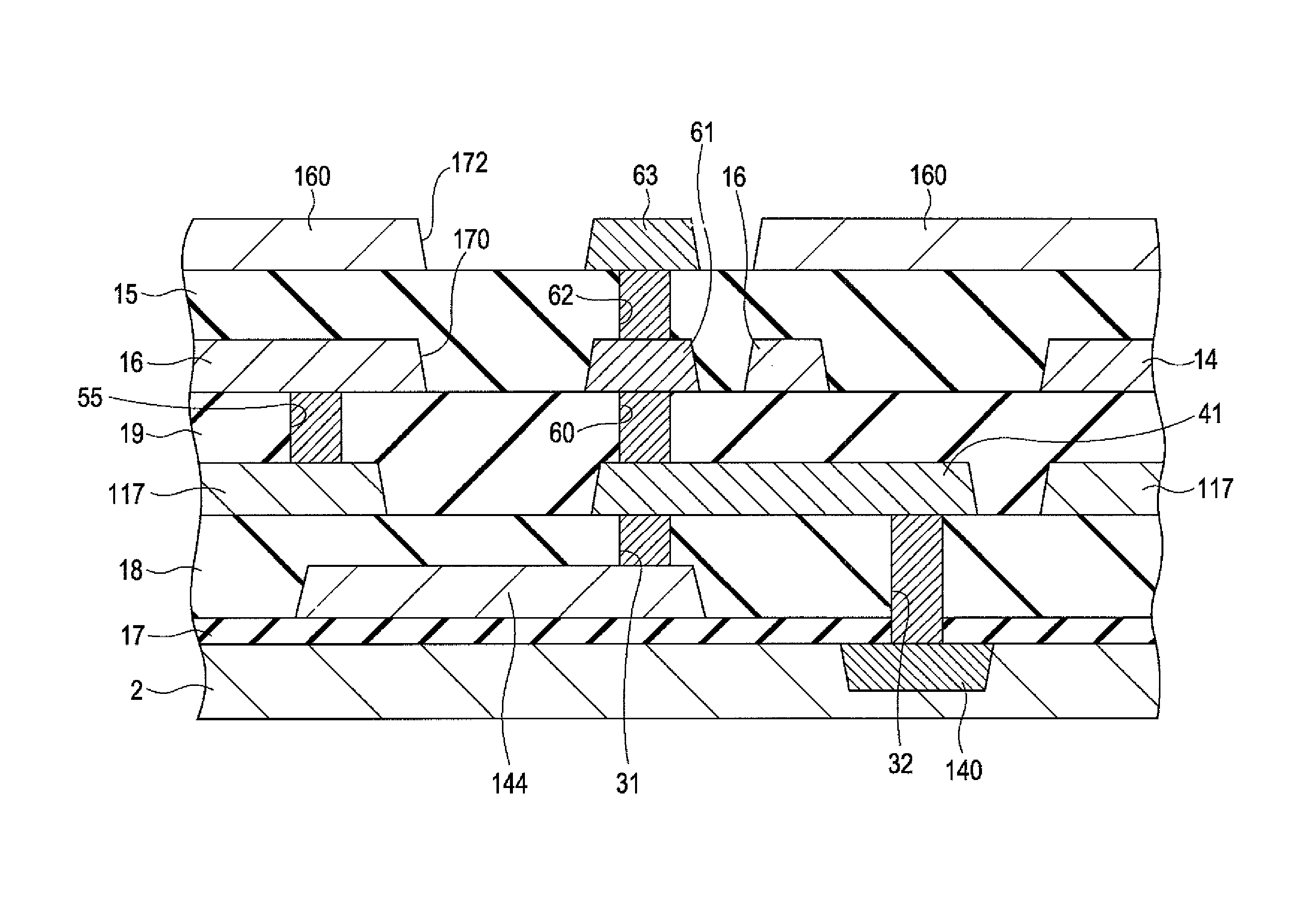
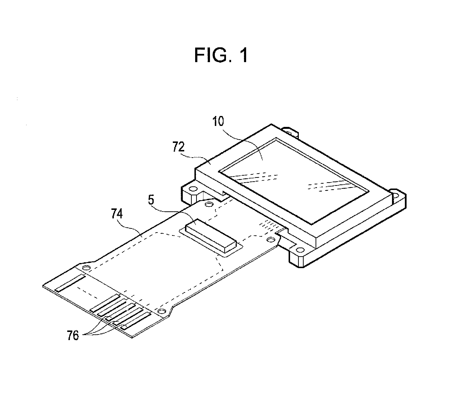
[0028]FIG. 1 is a perspective view illustrating a configuration of an electro-optical device 10 according to an embodiment of the invention. The electro-optical device 10 is a microdisplay that displays an image in a head-mounted display (HMD), for example. The electro-optical device 10, details of which will be described below, is an organic electroluminescent (EL) device in which a plurality of pixel circuits, driving circuits for driving the pixel circuits, and other components are formed in a silicon substrate, for example. An OLED, which is an exemplary emitting element, is used in the pixel circuit. The electro-optical device 10 is mounted in a frame-shaped case 72 having an opening for a display section. One end of a flexible printed circuit (FPC) substrate 74 is connected to the electro-optical device 10. A control circuit 5 of a semiconductor chip is mounted on the FPC substrate 74 using a chip-on-film (COF) technology. The FPC substrate 74 is provided with a plurality of t...


PUM


Abstract

An electro-optical device includes a scanning line and a data line intersecting each other, a pixel circuit provided at a position corresponding to an intersection of the scanning line and the data line, and a power supply wiring line that supplies a given potential. The pixel circuit includes a light emitting element and a driving transistor configured to control a current flowing through the light emitting element. A gate electrode of the driving transistor is electrically connected via a first relay electrode to a given node. The first relay electrode is formed in the same layer as the power supply wiring line and the data line. The first relay electrode is surrounded on at least three sides by the power supply line.

Description

BACKGROUND[0001]1. Technical Field[0002]The present invention relates to an electro-optical device and an electronic apparatus capable of reducing degradations in image quality associated with variations in the potential of data lines.[0003]2. Related Art[0004]Various types of electro-optical devices using light emitting elements such as organic light emitting diodes (hereinafter referred to as “OLEDs”) have recently been proposed. In the configuration of such an electro-optical device, typically, pixel circuits including the light emitting elements mentioned above, transistors, and other components are arranged at positions corresponding to intersections of scanning lines and data lines, and the pixel circuits are provided so as to correspond to pixels of an image to be displayed. A pixel circuit using an OLED typically includes a write transistor that determines whether or not a data signal is able to be input from a data line, a driving transistor that determines, on the basis of...

Claims


Application Information

Patent Timeline
Patent Type & Authority Patents(United States)
IPC IPC(8): H01L33/00H01L27/12H01L27/32
CPCH01L33/0041H01L27/3276H01L27/124G09G3/3208H10K59/131G09F9/301G09G3/30H10K59/123H10K59/121H10K50/11H10K59/1213H10K59/1216
Inventor KITAZAWA, TAKAYUKINOMURA, TAKESHI
Owner SEIKO EPSON CORP
Why Eureka
Try Eureka