Multi-beam semiconductor laser device

a laser device and semiconductor technology, applied in the direction of lasers, semiconductor laser arrangements, semiconductor lasers, etc., can solve problems such as thermal stress, and achieve the effect of suppressing the deterioration of element characteristics and beam pitch

Active Publication Date: 2016-01-05
USHIO OPTO SEMICON
View PDF16 Cites 1 Cited by
  • Summary
  • Abstract
  • Description
  • Claims
  • Application Information

AI Technical Summary

Benefits of technology

[0010]The multi-beam semiconductor laser element having the ridge structure and the bank structure is examined. A ridge formed above the light emitting portion is referred to as “light emitting ridge portion”. A pair of bank portions is formed on both sides of the light emitting ridge portion, and a unit of the light emitting ridge portion and the pair of bank portions is repeatedly arranged to realize the multi-beam semiconductor laser element for emitting multiple beams. In order to suppress cross talk generated between neighboring beams, it is desired to arrange an isolation trench between a bank portion of one unit and a neighboring bank portion of another unit. Further, by using the technology disclosed in JP 2011-108932 A, a height of an upper surface of a conductor formed on an upper part of one of the pair of bank portions is set to be larger than a height of an upper surface of a conductor formed on an upper part of the light emitting ridge portion. This multi-beam semiconductor laser element does not impair conductivity or heat dissipation and has stable polarization angle characteristics without requiring high positional accuracy in a step of mounting the laser chip on the submount.
[0016]The semiconductor laser element having the ridge structure has a simpler structure than other kinds of semiconductor elements, and hence has an advantage in that the number of steps in a multilayer growth process can be reduced. However, because the semiconductor laser element having the ridge structure has a simple structure, the light emitting ridge portion 102, which is important as a semiconductor laser function, is easily damaged mechanically due to handling or contact with a jig or tool in a manufacturing process. If the light emitting ridge portion, which is an important part having a role of guiding and amplifying the laser beam, is damaged, the laser cannot oscillate or is decreased in optical output.
[0017]The present invention has been made in view of the above-mentioned problems, and it is an object of the present invention to provide a semiconductor laser element and a semiconductor laser device in which deterioration of element characteristics is suppressed even when the beam pitch is reduced.
[0022](5) In the semiconductor laser element according to Item (4), in the one of the pair of neighboring ones of the plurality of light emitting ridge portions, an electrode formed above the first ridge semiconductor layer may be prevented from reaching the front end surface.
[0028]According to one embodiment of the present invention, the semiconductor laser element and the semiconductor laser device are provided, in which deterioration of element characteristics is suppressed even when the beam pitch is reduced.

Problems solved by technology

However, because there is a difference in linear expansion coefficient between the semiconductor material of the laser chip and the submount material, thermal stress may occur when the device bonded at high temperature is rapidly cooled to room temperature.
If the polarization angle of the laser beam is increased, when an optical component (lens or the like) having polarization angle dependence in optical characteristics is used, there occurs a malfunction such as a variation of a laser beam optical path or transmitted light intensity.

Method used


Image

  • Multi-beam semiconductor laser device
  • Multi-beam semiconductor laser device
  • Multi-beam semiconductor laser device

Examples


first embodiment

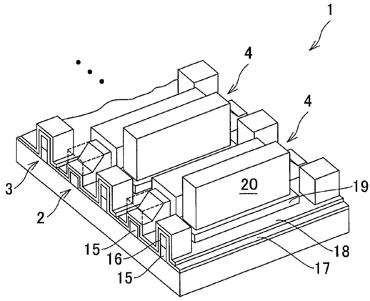
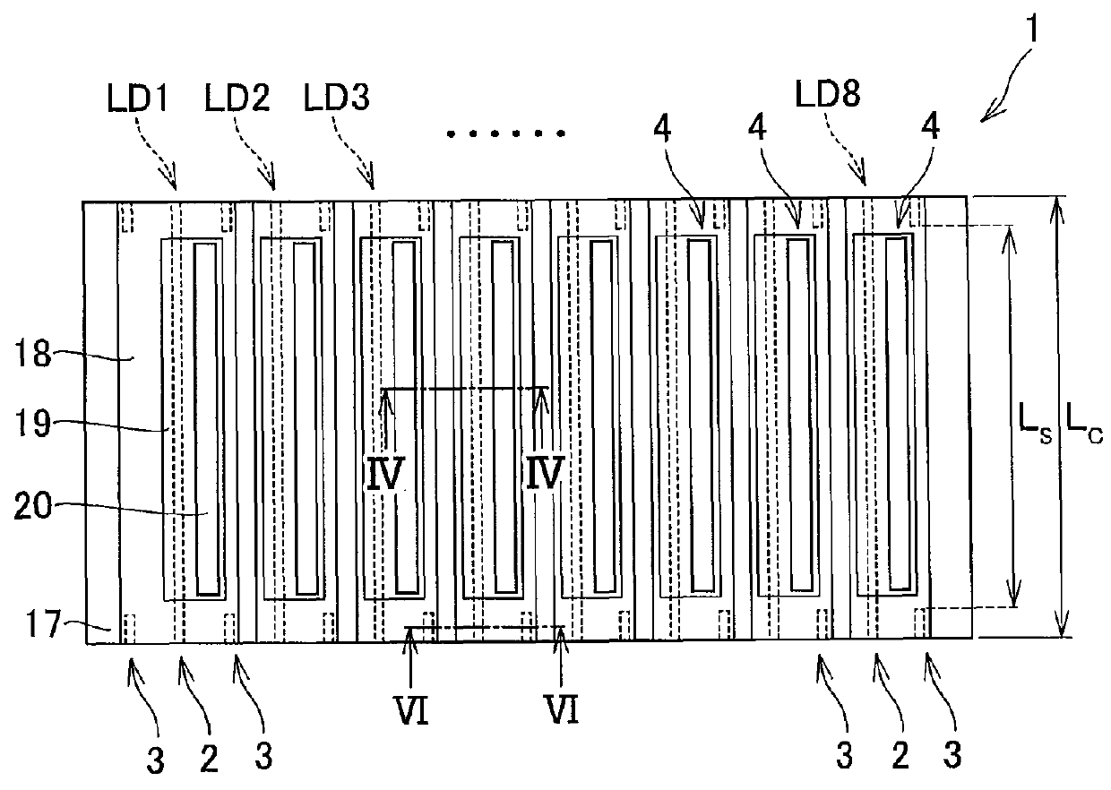
[0046]FIG. 1 is a perspective view illustrating a structure of a semiconductor laser element 1 according to a first embodiment of the present invention, and FIG. 2 is a top view illustrating the structure of the semiconductor laser element 1 according to this embodiment. The semiconductor laser element 1 according to this embodiment is a multi-beam semiconductor laser element in 660 nm band including eight light emitting ridge portions 2, and a semiconductor laser device according to this embodiment includes the semiconductor laser element 1 according to this embodiment.

[0047]The semiconductor laser element 1 includes short ridge portions 3 close to individual LD facets on both sides. As used herein, the LD facets are end surfaces arranged at both ends of the light emitting ridge portion 2 extending in a vertical direction of FIG. 2. A front LD facet is an end surface on a signal light emitting side, and a rear LD facet is an end surface on a monitor light emitting side. Supposing t...

second embodiment

[0087]A semiconductor laser element according to a second embodiment of the present invention is different from the semiconductor laser element according to the first embodiment in the structure of the short ridge portion 3, but the other parts are the same. FIG. 7 is a top view illustrating a structure of the semiconductor laser element 1 according to this embodiment.

[0088]The end of the short ridge portion 3 (second ridge semiconductor layer or third ridge semiconductor layer) on the LD facet side of the semiconductor laser element 1 according to the first embodiment reaches the LD facet. The end is aligned with the LD facet. However, this structure is not a limitation. The end of the short ridge portion 3 on the LD facet side of the semiconductor laser element 1 according to this embodiment is positioned inside the LD facet. It is desired that the distance between the end and the LD facet be 1 μm to 30 μm, for example.

[0089]In this embodiment, the height of the end of the short r...

third embodiment

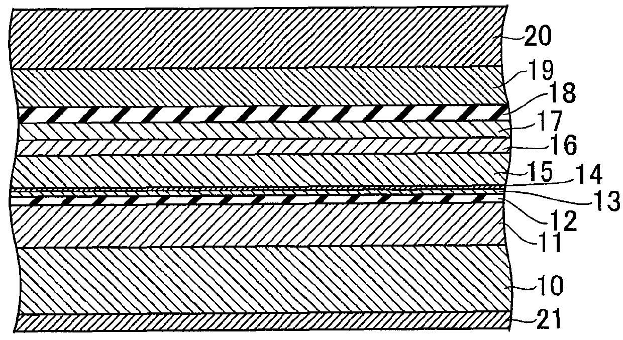
[0091]A semiconductor laser element according to a third embodiment of the present invention is different from the semiconductor laser element according to the first or second embodiment in the structure of the light emitting ridge portion 2 in the vicinity of the LD facet, but the other parts are the same. FIG. 8 is a top view illustrating a structure of the semiconductor laser element 1 according to this embodiment, and FIG. 9 is a cross-sectional view of the semiconductor laser element 1 according to this embodiment. FIG. 9 illustrates a cross section taken along the line IX-IX of FIG. 8. In the semiconductor laser element 1 according to this embodiment, in the vicinity of the LD facet, the p-type electrode layer 18 is removed from the light emitting ridge portion 2. In other words, the p-type electrode layer 18 formed on the upper part of the light emitting ridge portion 2 (above the first ridge semiconductor layer) does not reach the LD facet. FIG. 9 illustrates the region from...


PUM


Abstract

Provided is a multi-beam semiconductor laser device in which deterioration of element characteristics is suppressed even when a beam pitch is reduced. The multi-beam semiconductor laser device includes: a first semiconductor multilayer in which a plurality of semiconductor layers are laminated; a plurality of light emitting ridge portions that are formed on the first semiconductor multilayer; a support electrode portion formed in a region between a pair of neighboring light emitting ridge portions; and a front ridge portion formed on the front side of the support electrode portion. The support electrode portion is electrically connected to one of the pair of neighboring light emitting ridge portions. The support electrode portion is higher than the one light emitting ridge portion. An end of the front ridge portion on the front end surface side is higher than the one light emitting ridge portion at the front end surface.

Description

CROSS-REFERENCE TO RELATED APPLICATION[0001]The present application claims priority from Japanese application JP 2013-173112 filed on Aug. 23, 2013, the content of which is hereby incorporated by reference into this application.BACKGROUND OF THE INVENTION[0002]1. Field of the Invention[0003]The present invention relates to a semiconductor laser element and a semiconductor laser device including the same, and more particularly, to a technology for reducing a beam pitch of a multi-beam semiconductor laser element.[0004]2. Description of the Related Art[0005]For instance, a semiconductor laser device used for a light source of an image printing apparatus such as a laser printer or a copying machine is equipped with a semiconductor laser element (laser chip) in which a light emitting portion is formed on a semiconductor substrate (hereinafter referred to simply as “substrate”). In particular, a multi-beam semiconductor laser element in which a plurality of light emitting portions are fo...

Claims


Application Information

Patent Timeline
Patent Type & Authority Patents(United States)
IPC IPC(8): H01S5/22H01S5/40H01S5/34H01S5/343H01S5/42H01S5/10H01S5/022H01S5/042
CPCH01S5/22H01S5/0224H01S5/02256H01S5/343H01S5/3407H01S5/40H01S5/4031H01S5/02272H01S5/0425H01S5/1082H01L2224/16225H01S5/04254H01S5/04256H01S5/0234H01S5/02345H01S5/02355H01S5/0237
Inventor INOUE, YUTAKAHARA, HIDEKIUSUDA, SHUICHI
Owner USHIO OPTO SEMICON
Why Eureka
Try Eureka