Power transistor gate driver

a technology of power transistors and gate terminals, applied in transistors, electronic switching, pulse techniques, etc., can solve the problem of not being able to supply further charging current to the gate terminals on the charging path, and achieve the effect of high voltage devices, robustness and low cos

Active Publication Date: 2016-01-05
INFINEON TECH AUSTRIA AG
View PDF5 Cites 10 Cited by
  • Summary
  • Abstract
  • Description
  • Claims
  • Application Information

AI Technical Summary

Benefits of technology

[0012]In one embodiment, a predetermined threshold voltage is provided to the controller to set the first voltage and the controller is adapted to control the supply of charging currents to the gate terminal through the first and second charging paths by comparing the gate voltage of the power transistor with the predetermined threshold voltage. The predetermined threshold voltage may for example be derived from a drain voltage of a power transistor electrically coupled to the first charging path. The predetermined threshold voltage may be set to a voltage level about one MOS threshold voltage below a drain voltage of the power transistor. In practice, the predetermined threshold voltage will then typically be situated between 0.5 and 1.0 V below a drain voltage of the power transistor. This embodiment allows the first voltage of a given gate driver to be conveniently adapted to the actual voltage level of its associated power transistor.
[0020]The load driving assembly may be connected directly to a loudspeaker load coupled to the output terminal. The load driving assembly may for example comprise between 2 and 8 cascaded power transistors each having its drain and gate terminals coupled to a separate gate driver. According to a preferred embodiment of the load driving assembly, the second voltage supplies of the plurality of gate drivers are electrically connected to a common charge pump capacitor of the second voltage supply. This embodiment allows the plurality of second charging paths to receive their respective charging currents from a single shared high voltage supply requiring only a single capacitor. Consequently, since a typical load driving assembly may comprise more than 4 cascaded power transistor such as 6, 8 or even more, the ability to share the second voltage from a single capacitor based high voltage supply reduces the need for bootstrap capacitor to drive the gate terminals of the power transistors. So despite the common charge pump capacitor may have a considerable capacitance value such as between 10 nF and 100 nF, which requires it to be an external component to the load driving assembly, only a single capacitor component is required.
[0022]According to yet another advantageous embodiment of the invention, the load driving assembly is formed or integrated on a semiconductor substrate such as CMOS integrated circuit, preferably in a semiconductor process that supports high voltage devices. The semiconductor substrate provides a robust and low-cost single chip solution for the manufacture of the load driving assembly which is particularly well-suited for high-volume consumer oriented audio applications, such as TV sets, mobile phones and MP3 players, where cost is an essential parameter. The semiconductor substrate preferably comprises a voltage supply terminal providing electrical connection to the external charge pump capacitor acting as an energy reservoir for the second voltage supply.

Problems solved by technology

At that condition, the first charging path is unable of supplying further charging current to the gate terminal due to a reversal of the flow of charging current.

Method used


Image

  • Power transistor gate driver
  • Power transistor gate driver
  • Power transistor gate driver

Examples


Embodiment Construction

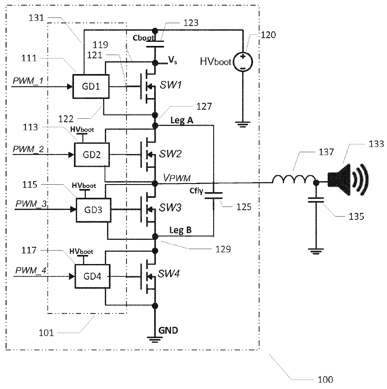
[0029]FIG. 1 illustrates schematically a load driving assembly 100 connected to a loudspeaker load 133. The load driving assembly 100 comprises a gate driving circuit 101 comprising four individual gate drivers 111, 113, 115, 117 in accordance with a preferred embodiment of the present invention. Each of the gate drivers has an output terminal electrically connected to a gate terminal of one of NMOS transistors SW1, SW2, SW3, SW4. The NMOS transistors SW1, SW2, SW3, SW4 are coupled in cascade between a first or positive DC supply voltage VS and a second DC supply voltage in form of ground, GND. The cascaded NMOS transistors SW1, SW2, SW3, SW4 form a load driver for the loudspeaker load 133 coupled to an output terminal VPWM of the load driver through a load inductor 137 and a load capacitor 135. The combined operation of the load capacitor and load inductor 135, 137, respectively, is to provide lowpass filtering of a multi-level pulse width modulated output signal waveform provided ...


PUM


Abstract

The present invention relates to a gate driver for a power transistor comprising a first charging path operatively connected between a first voltage supply and a gate terminal of the power transistor for charging the gate terminal to a first gate voltage. A second charging path is connectable between the gate terminal of the power transistor and a second supply voltage to charge the gate terminal from the first gate voltage to a second gate voltage larger or higher than the first gate voltage. A voltage of the second voltage supply is higher than a voltage of the first voltage supply.

Description

[0001]The present invention relates to a gate driver for a power transistor comprising a first charging path operatively connected between a first voltage supply and a gate terminal of the power transistor for charging the gate terminal to a first gate voltage. A second charging path is connectable between the gate terminal of the power transistor and a second supply voltage to charge the gate terminal from the first gate voltage to a second gate voltage larger or higher than the first gate voltage. A voltage of the second voltage supply is higher than a voltage of the first voltage supply. Another aspect of the invention relates to a load driving assembly comprising a plurality of gate drivers electrically coupled to respective ones of a plurality of power transistors. The load driving assembly may be utilized in various power amplification applications such as class D audio amplifiers.BACKGROUND OF THE INVENTION[0002]Gate drivers for power transistors of a power or output stage of...

Claims


Application Information

Patent Timeline
Patent Type & Authority Patents(United States)
IPC IPC(8): H03F3/217H03K17/06H03K17/687H02M1/08
CPCH03K17/687H02M1/08H03F3/2171H03F3/2173H03K17/063H03K17/6871H02M7/4837
Inventor HOYERBY, MIKKELJAKOBSEN, JORGEN KRAGH
Owner INFINEON TECH AUSTRIA AG
Why Eureka
Try Eureka