Charge pump circuits

a technology of pump circuits and discharge pumps, applied in the direction of corona discharge, process and machine control, instruments, etc., can solve the problems of normal applied voltages and damage to transistors, and achieve the effect of minimising the chance of transistors exceeding their breakdown voltage and minimizing voltage differences

Active Publication Date: 2014-06-10
CIRRUS LOGIC INC
View PDF6 Cites 5 Cited by
  • Summary
  • Abstract
  • Description
  • Claims
  • Application Information

AI Technical Summary

Benefits of technology

[0018]A leakage element is an element that, whilst generally having the property of preventing current flow (at least in one direction) nevertheless allows a small current to leak through the barrier presented by the leakage element. The leakage elements used in the present invention are thus arranged to allow a leakage current to flow, i.e. a current which, in normal operating conditions is not significant enough to prevent satisfactory operation of the charge pump but, in the event of a developing voltage transient, allows sufficient current to flow to maintain a safe applied voltage. The skilled person will appreciated that leakage elements are high impedance elements, at least as regards current flow from a higher voltage to a lower voltage stage of the charge pump, so as to prevent excess current flow in normal operation.
[0019]The leakage element is preferably adapted so as to minimise the chance of the transistor exceeding its breakdown voltage. The leakage element is therefore conveniently adapted to allow a leakage current to flow at a voltage below the breakdown voltage of the transistor, i.e. it is adapted to prevent a voltage difference developing across the transistor which is greater than the breakdown voltage of the transistor. The transistors may, as described above, be relatively low voltage elements and have a breakdown voltage less than the voltage output of the charge pump circuit.
[0020]The leakage element may therefore be adapted to allow a leakage current of more than 100 pA or more than 1 nA or more than 10 nA or more than 100 nA at a voltage less than the breakdown voltage of the transistor. The leakage element may be adapted to allow a leakage current of around 1 μA to flow. For instance if the safe operating voltage of the transistor was around 3V for example, the leakage element may be adapted to allow a leakage current of greater than 1 nA or greater than 10 nA or greater than 100 nA or around 1 μA to flow at a voltage around 3V. Such a leakage current would quickly drain charge from the high voltage stage and maintain charge on the low voltage stage so as to minimise the voltage difference and hence prevent the voltage across the transistor from exceeding the breakdown voltage.
[0032]In another aspect of the present invention there is provided a method of protecting a circuit component in a charge pump from voltage levels higher than normal operating voltages comprising the step of arranging a leakage element in parallel with said circuit component. The circuit component may comprise a transistor and the transistor may have a breakdown voltage less than the voltage output of the charge pump circuit. The leakage element may be adapted to prevent a voltage across the transistor which is greater than the breakdown voltage of the transistor

Problems solved by technology

As described above a charge pump circuit may be designed using transistors that are capable of operating at the normal operating voltages of the charge pump, but that certain events may lead to voltage transients which generate greater than normal applied voltages that may damage the transistors.

Method used


Image

  • Charge pump circuits
  • Charge pump circuits
  • Charge pump circuits

Examples


Embodiment Construction

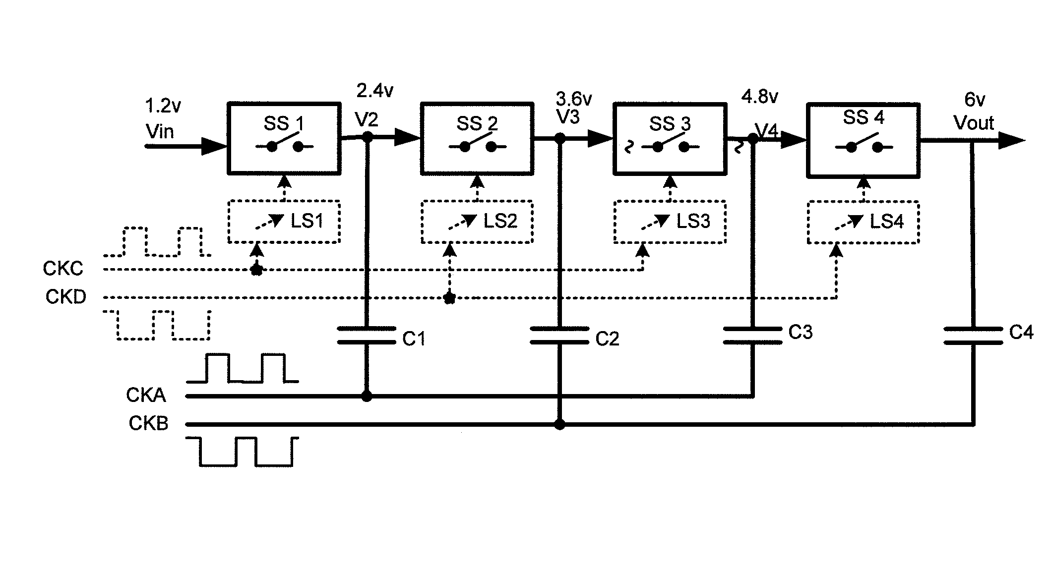
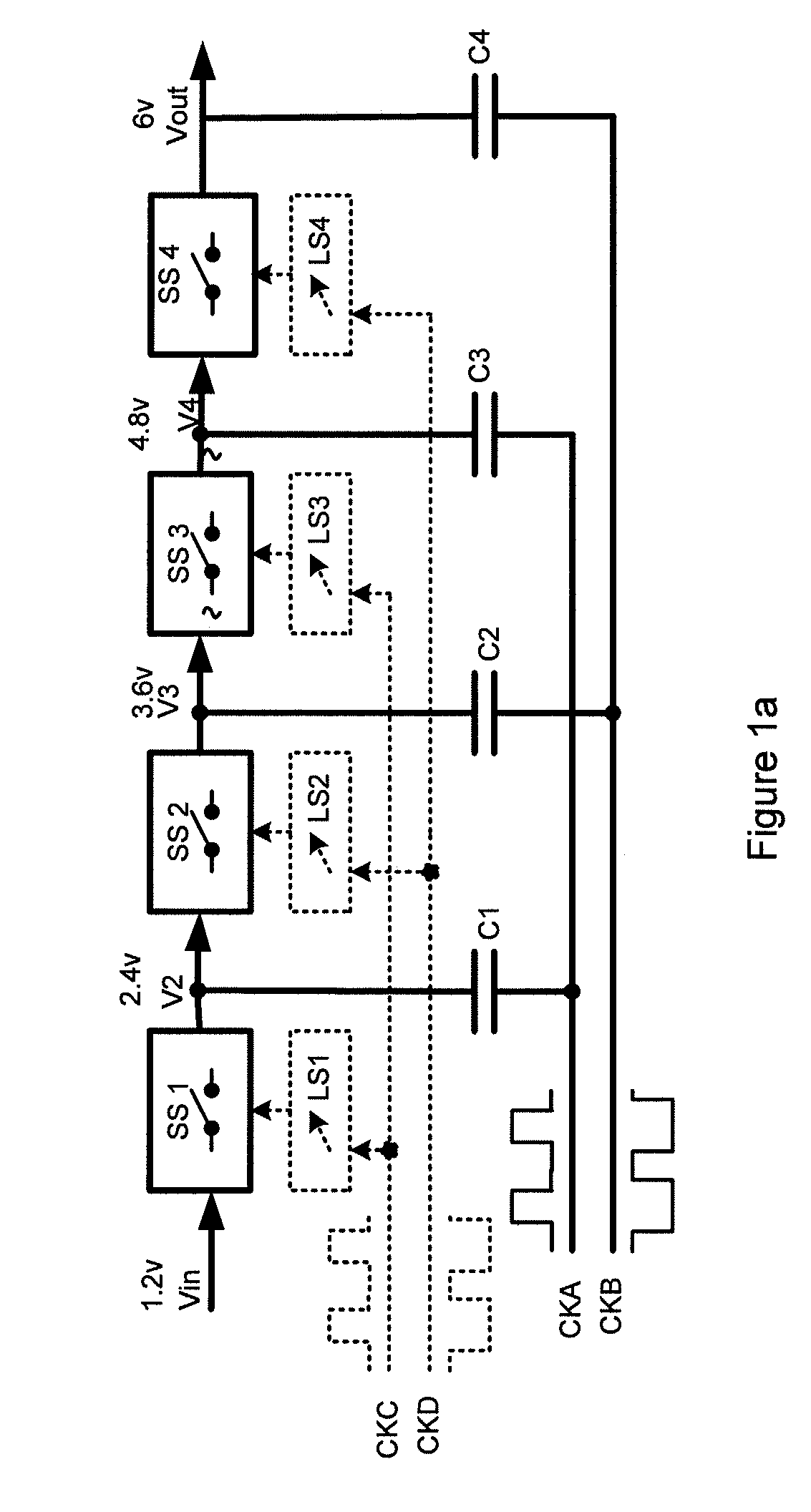
[0049]FIG. 2 shows a charge pump architecture embodiment according to an aspect of the invention. The circuit operates in the same manner, and is similar in arrangement to a convention charge pump circuit such as that shown in FIG. 1, but with the addition of leakage elements, diode clamp devices D1 to D4, across consecutive switch blocks SS1 to SS4, between consecutive pump capacitors C1 to C4. The diodes clamp devices each comprise a diode arranged to be reverse biased in terms of current flow from a higher voltage stage of the charge pump to a lower voltage stage of the charge pump.

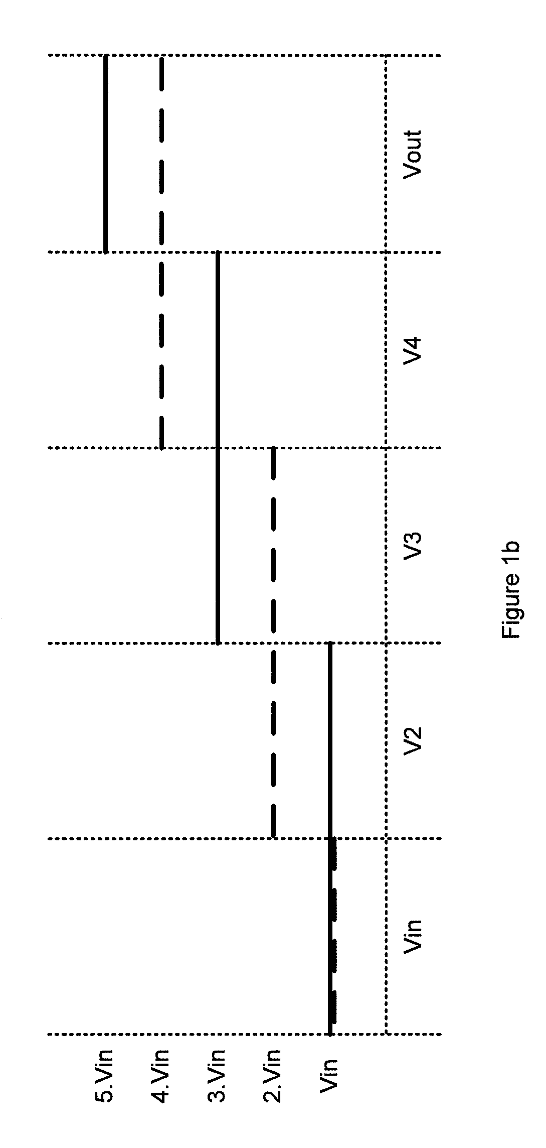
[0050]As described above, in normal operation, the voltage difference across each switching stage will be either zero or 2Vin. Thus, except for brief transients, these diodes will either be at zero bias or reverse biased by 2.Vin. In the event of a power down the capacitors will begin to discharge. In the example described above in relation to FIG. 1c a leakage current associated with capacitor C3 caus...


PUM


Abstract

Charge pump circuits having circuit components such as transistors which may be damaged by voltage transients greater than the normal operating voltage levels of the charge pump circuit, such as may be experienced during powering down. The circuit components to be protected are connected in parallel with a leakage element arranged to have a leakage current that is small enough during normal operation to allow the charge pump to operate effectively but which is large enough, during development of a voltage transient, to prevent excess voltage levels being achieved. The leakage element may have a significant leakage current at a voltage less than the breakdown voltage of the circuit component. Suitable leakage elements are poly diodes.

Description

BACKGROUND OF THE INVENTION[0001]1. Field of the Invention[0002]The present invention relates to charge pump circuits having leakage elements arranged to act as protective shunt elements across low-voltage semiconductor devices, and in particular, but not exclusively, to such circuits having high impedance diodes with current leakage characteristics.[0003]2. Description of the Related Art[0004]Capacitive charge pumps and their use in generating higher voltages from a lower-voltage power supply are well known. Their use is increasing due to the proliferation of battery-powered consumer gadgets such as MP3 players and mobile phones. For example one use is to provide a voltage for MEMS microphone transducers, where a 12V transducer bias voltage may need to be derived from a supply as low as 1.5V.[0005]FIG. 1a illustrates a general capacitive charge pump comprising four pumped capacitors C1 to C4 interposed between switching stages SS1 to SS4. In operation, the voltages on the bottom pl...

Claims


Application Information

Patent Timeline
Patent Type & Authority Patents(United States)
IPC IPC(8): H04R3/00
CPCH02M3/073H02M1/32H02M3/07
Inventor PENNOCK, JOHN LAURENCEBOWLERWELL, JOHN BRUCE
Owner CIRRUS LOGIC INC
Why Eureka
Try Eureka