Display device and electronic device

a technology of electronic devices and display devices, applied in semiconductor devices, instruments, optics, etc., can solve the problems of lowering display quality, contact failure between transparent electrodes and reflective electrodes, lowering reflectivity, etc., and achieves high reflectivity , reduce contact failure, the effect of high reflectivity

Active Publication Date: 2016-01-26
SEMICON ENERGY LAB CO LTD
View PDF13 Cites 1 Cited by
  • Summary
  • Abstract
  • Description
  • Claims
  • Application Information

AI Technical Summary

Benefits of technology

[0010]In view of the above problems, an object of one embodiment of the present invention is to provide a novel display device capable of excellent display. Another object of one embodiment of the present invention is to provide a novel display device of which productivity is improved. Another object of one embodiment of the present invention is to provide a novel display device capable of excellent reflective display. Another object of one embodiment of the present invention is to provide a novel display device with a COA structure that is capable of excellent reflective display.
[0013]As described above, the display device of one embodiment of the present invention includes a reflective electrode layer that is formed on the same plane as a source electrode layer and a drain electrode layer of a transistor. The reflective electrode layer in a reflective region is a conductive layer with high reflectivity. In a contact region between the transistor and a pixel electrode layer, an anti-oxidation conductive layer is formed over the conductive layer with high reflectivity. The anti-oxidation conductive layer can reduce contact failures between the pixel electrode layer and the source and drain electrode layers.
[0014]In other words, in the display device of one embodiment of the present invention, the conductive layer with high reflectivity is used in the reflective region, and the anti-oxidation conductive layer is used in the contact region between the transistor and the pixel electrode layer; thus, the display device is a novel display device which is capable of excellent reflective display and in which contact failures between a transistor and a pixel electrode layer are reduced.
[0015]In one embodiment of the present invention, a novel display device capable of excellent display can be provided. Further, in one embodiment of the present invention, a novel display device of which productivity is improved can be provided. Further, in one embodiment of the present invention, a novel display device capable of excellent reflective display can be provided. Further, in one embodiment of the present invention, a novel display device with a COA structure that is capable of excellent reflective display can be provided.

Problems solved by technology

In the structure disclosed in Patent Document 1, a color filter layer is formed directly on a metal layer serving as a reflective electrode; thus, in the case where a material with high reflectivity such as aluminum or an aluminum alloy is used for the metal layer, when the color filter layer is formed by a photolithography process, the metal layer is eroded by an alkaline developer during development of the color filter layer, which results in lowered reflectivity.
In addition, a transparent electrode that is used as one electrode of a liquid crystal element is directly connected to the metal layer serving as a reflective electrode; thus, oxidation of the metal layer causes a contact failure between the transparent electrode and the reflective electrode.
Placing such a transparent conductive material at the outermost surface of the reflective layer causes problems (for example, reflectivity is lowered and reflected light is colored depending on incident light wavelength) and results in lowered display quality.
In addition, in the structure disclosed in Patent Document 2, the reflective layer and a color filter layer need to be formed over a TFT substrate and there is a problem of low productivity.

Method used


Image

  • Display device and electronic device
  • Display device and electronic device
  • Display device and electronic device

Examples


embodiment 1

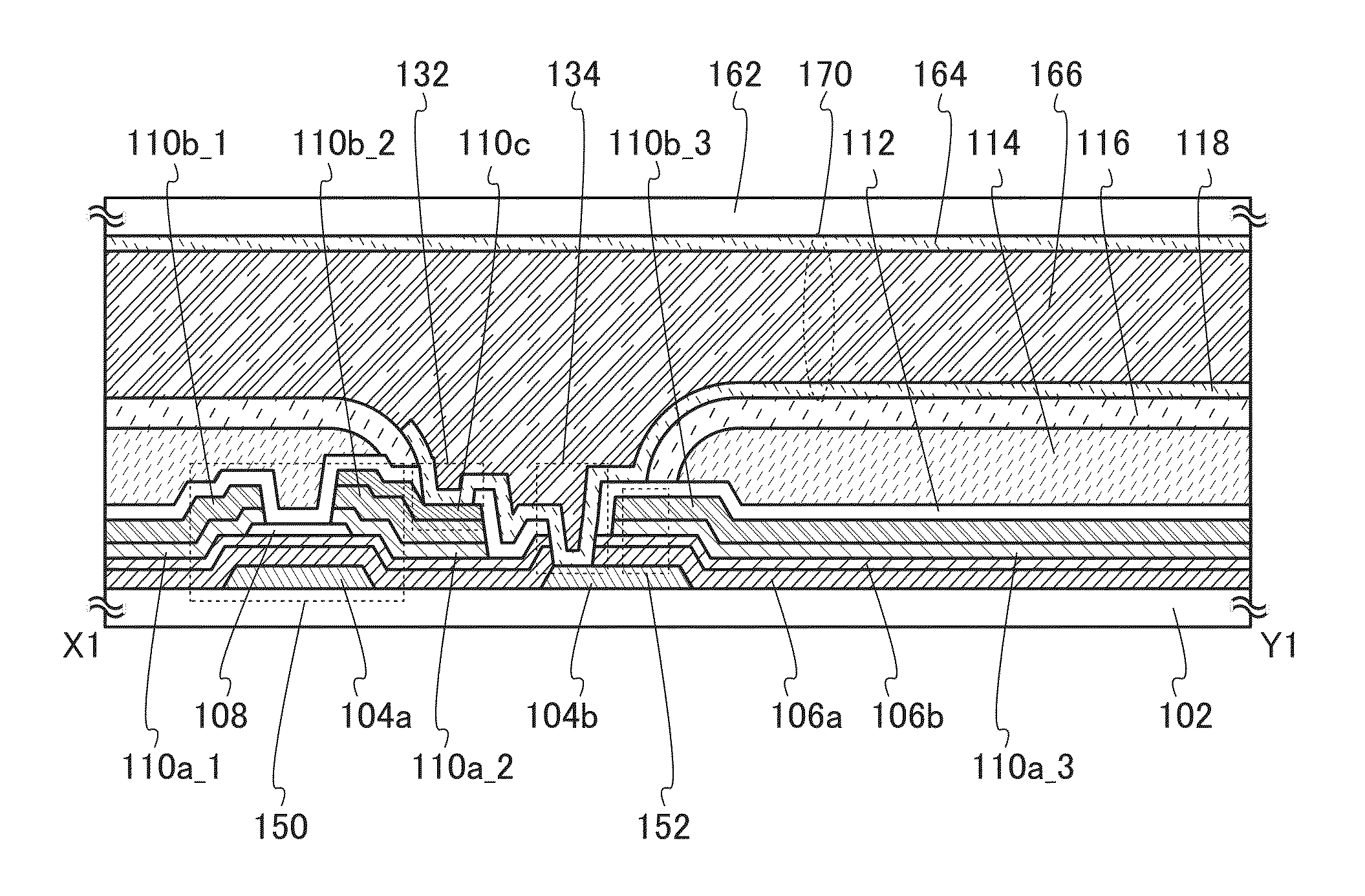
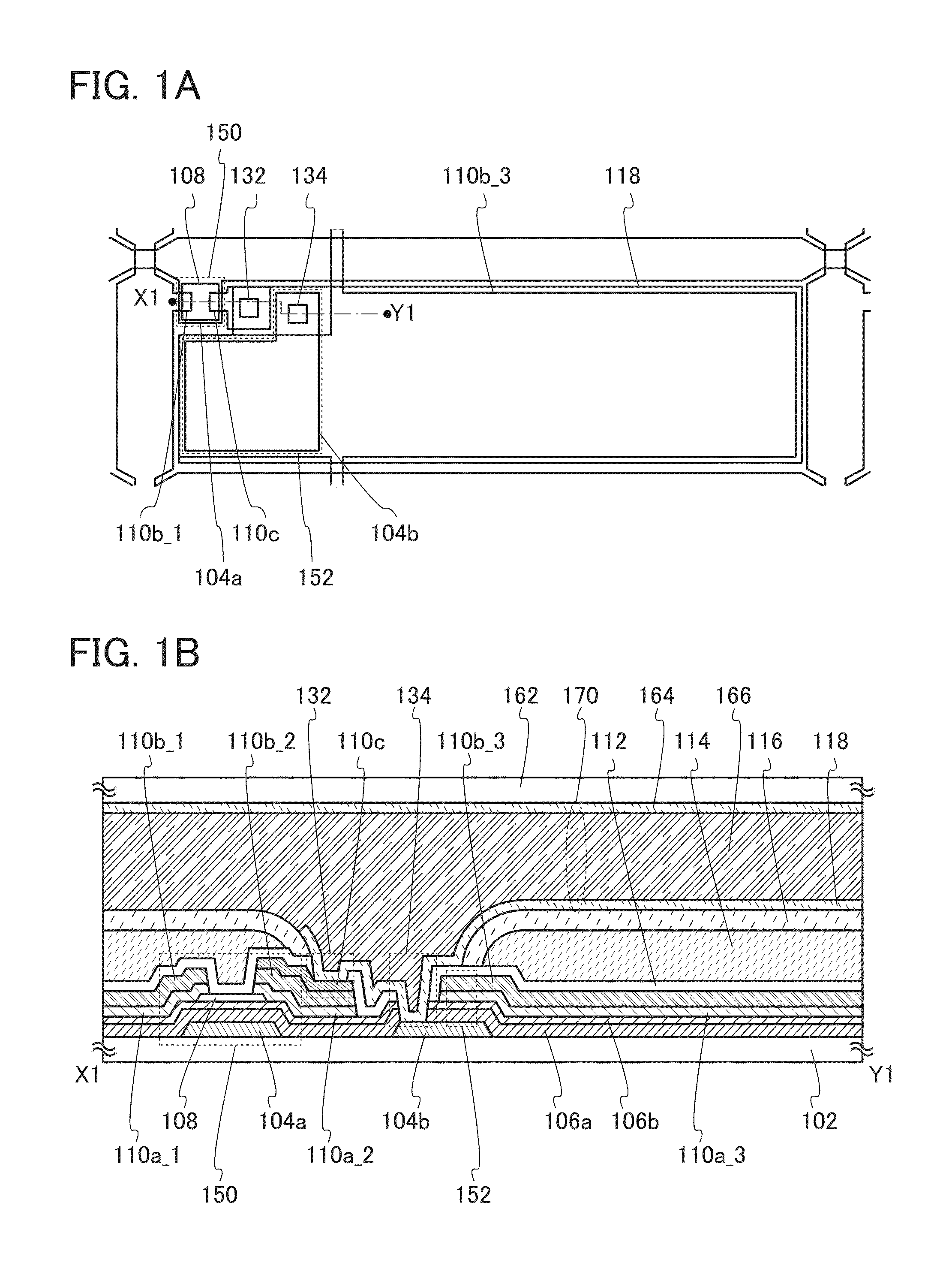
[0034]In this embodiment, a display device of one embodiment of the present invention will be described with reference to FIGS. 1A and 1B, FIGS. 2A to 2D, FIGS. 3A to 3D, and FIGS. 4A to 4C.

[0035]FIG. 1A is a top view of an example of a display device of one embodiment of the present invention. FIG. 1B is a cross-sectional view corresponding to a section plane taken along a dashed-dotted line X1-Y1 in FIG. 1A. In the top view of FIG. 1A, which shows part of a pixel portion in the display device, components such as a gate insulating layer and a coloring layer are partly omitted to avoid complexity.

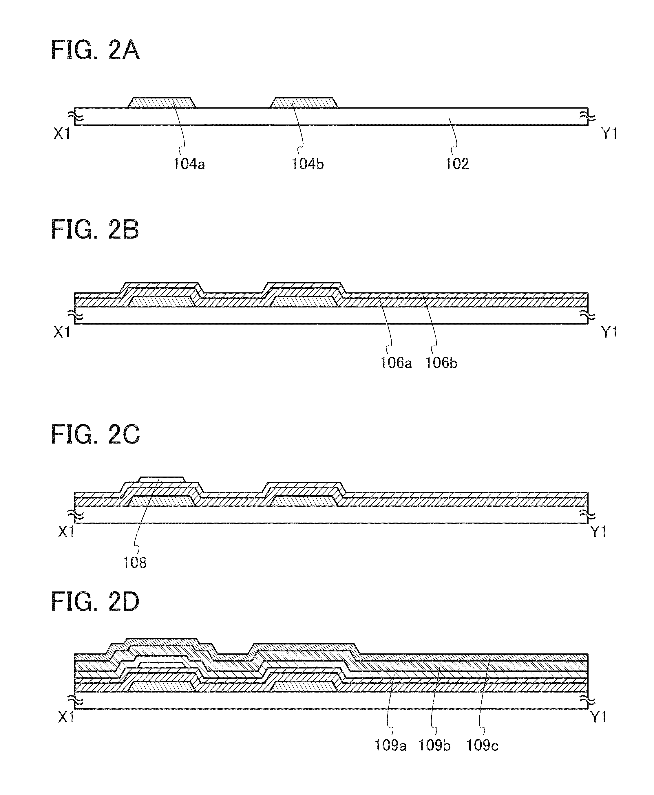
[0036]In FIG. 1A, a transistor 150 includes a conductive layer 104a serving as a gate electrode layer, the gate insulating layer (not illustrated in FIG. 1A), a semiconductor layer 108 where a channel region is formed, and a conductive layer 110b_1 and a conductive layer 110b_2 (not illustrated in FIG. 1A) that serve as a source electrode layer and a drain electrode layer. The semiconductor...

embodiment 2

[0102]In this embodiment, a modification example of the display device described in Embodiment 1 is described with reference to FIGS. 5A and 5B, FIGS. 6A to 6D, and FIGS. 7A to 7D. Note that portions having functions similar to those in Embodiment 1 are given the same reference numerals and detailed description thereof is omitted.

[0103]FIG. 5A is a top view of an example of a display device of one embodiment of the present invention. FIG. 5B is a cross-sectional view corresponding to a section plane taken along a dashed-dotted line X2-Y2 in FIG. 5A. In the top view of FIG. 5A, which shows part of a pixel portion in the display device, components such as a gate insulating layer and a coloring layer are partly omitted to avoid complexity.

[0104]In FIG. 5A, a transistor 160 includes the conductive layer 104a serving as a gate electrode layer, the gate insulating layer (not illustrated in FIG. 5A), the semiconductor layer 108 where a channel region is formed, and the conductive layers 11...

embodiment 3

[0141]In this embodiment, a modification example of the display device described in Embodiment 1 is described with reference to FIG. 8.

[0142]FIG. 8 is a cross-sectional view illustrating an example of a display device of one embodiment of the present invention.

[0143]The display device of one embodiment of the present invention in FIG. 8 includes a transistor 250 having a top-gate structure, unlike the display devices in Embodiments 1 and 2.

[0144]The transistor 250 includes a semiconductor layer 208 in which a channel region is formed, an insulating layer 206a and an insulating layer 206b serving as a gate insulating layer, a conductive layer 204 serving as a gate electrode layer, an insulating layer 221 and an insulating layer 223 serving as an interlayer insulating layer, and a conductive layer 210a_1, a conductive layer 210a_2, a conductive layer 210b_1, and a conductive layer 210b_2 serving as a source electrode layer and a drain electrode layer.

[0145]The display device in FIG. 8...


PUM

PropertyMeasurementUnit
sizesaaaaaaaaaa
sizesaaaaaaaaaa
sizesaaaaaaaaaa

Abstract

A novel display device capable of excellent reflective display is provided. The display device includes a transistor including a gate electrode layer, a gate insulating layer over the gate electrode layer, a semiconductor layer over the gate insulating layer, and a source electrode layer and a drain electrode layer over the gate insulating layer and the semiconductor layer; a reflective electrode layer on the same plane as the source electrode layer and the drain electrode layer; a coloring layer overlapping with the reflective electrode layer; a pixel electrode layer overlapping with the coloring layer; and an anti-oxidation conductive layer connected to one of the source electrode layer and the drain electrode layer. The pixel electrode layer is connected to the transistor through the anti-oxidation conductive layer.

Description

TECHNICAL FIELD[0001]One embodiment of the present invention relates to a semiconductor device, a display device, a light-emitting device, or an electronic device. One embodiment of the present invention relates to, for example, a reflective liquid crystal display device. One embodiment of the present invention relates to a reflective liquid crystal display device with a COA structure.[0002]Note that the term “display device” means a device including a display element. In addition, the display device also includes a driver circuit for driving a plurality of pixels, for example. Further, the display device includes a control circuit, a power supply circuit, a signal generation circuit, or the like formed over another substrate.BACKGROUND ART[0003]With the recent rapid spread of portable information terminals such as smartphones, improvement in their performance has progressed rapidly. Their screens have been increased in size and resolution, and some recent ones have resolutions as h...

Claims


Application Information

Patent Timeline
Patent Type & Authority Patents(United States)
IPC IPC(8): G02F1/136H01L27/12G02F1/1335G02F1/1343G02F1/1362
CPCH01L27/124G02F1/13439G02F1/133553G02F2001/136218G02F1/136218G02F1/133345G02F1/1368H01L29/41733H01L29/78618
Inventor NAKADA, MASATAKAMORI, HIDENORIOHTANI, HISASHI
Owner SEMICON ENERGY LAB CO LTD
Why Eureka
Try Eureka