Semiconductor device, manufacturing method of semiconductor device, semiconductor wafer, and electronic equipment

a semiconductor and manufacturing method technology, applied in the direction of semiconductor/solid-state device details, semiconductor/solid-state device testing/measurement, radiation controlled devices, etc., can solve the problem of the method of connecting the contact pads from the outsid

Active Publication Date: 2016-02-16
SONY CORP
View PDF19 Cites 7 Cited by
  • Summary
  • Abstract
  • Description
  • Claims
  • Application Information

AI Technical Summary

Benefits of technology

[0016]According to the present technology, miniaturization of a semiconductor device and electronic equipment is possible. Further, it is possible to provide a manufacturing method of a semiconductor device that can be miniaturized.

Problems solved by technology

Meanwhile, in the backside illumination type solid state imaging device, since there are no contact pads on the upper surface, a method of connecting the contact pads from the outside is a problem.

Method used


Image

  • Semiconductor device, manufacturing method of semiconductor device, semiconductor wafer, and electronic equipment
  • Semiconductor device, manufacturing method of semiconductor device, semiconductor wafer, and electronic equipment
  • Semiconductor device, manufacturing method of semiconductor device, semiconductor wafer, and electronic equipment

Examples


first embodiment

2. First Embodiment

Semiconductor Device and Semiconductor Wafer

[Schematic Configuration of Solid State Imaging Device]

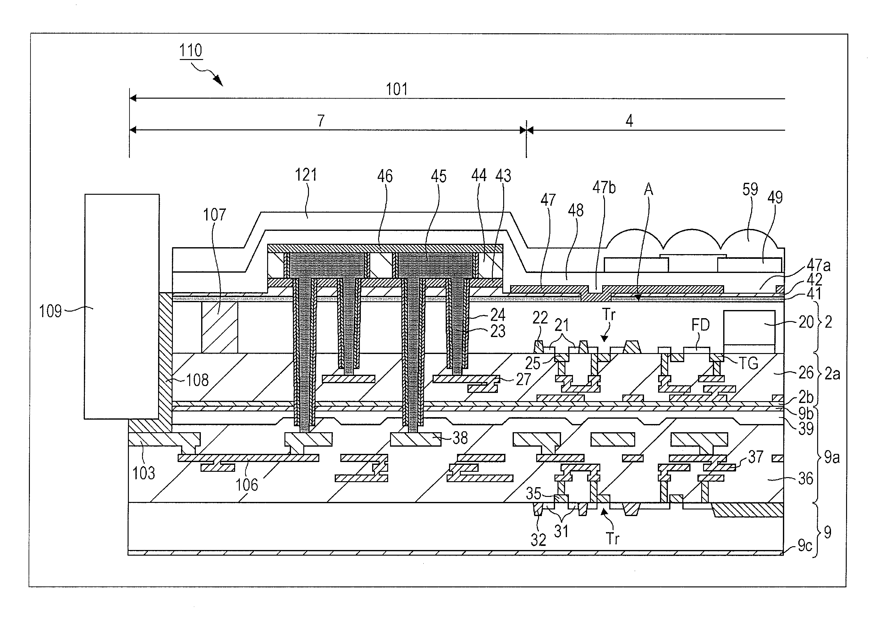
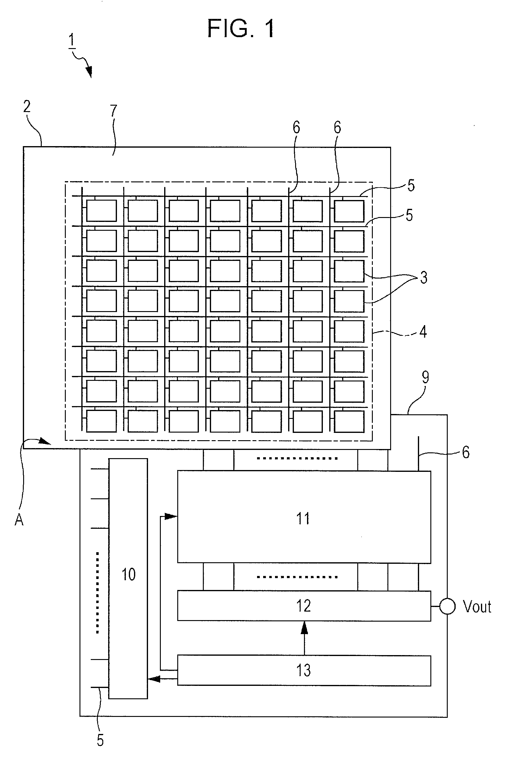
[0094]FIG. 1 illustrates a schematic configuration of a backside illumination type solid state imaging device of a three-dimensional structure, as an example of a semiconductor device to which the present technology is applied. A solid state imaging device 1 illustrated in FIG. 1 includes a sensor board 2 in which photoelectric conversion units are arranged and formed, and a circuit board 9 which is attached to the sensor board 2 in a state of being laminated.

[0095]The sensor board 2, in which one surface is a light receiving surface A, includes a pixel region 4 in which a plurality of pixels 3 including photoelectric conversion units are two-dimensionally arranged with respect to the light receiving surface A. In the pixel region 4, a plurality of pixel driving lines 5 are wired in a row direction, a plurality of vertical signal lines 6 are wired in a column directi...

second embodiment

4. Second Embodiment

Semiconductor Device and Semiconductor Wafer

[0175]Next, a second embodiment of the semiconductor device and the semiconductor wafer will be described. In the second embodiment, only the configuration regarding the external connection terminal of the semiconductor device is changed from the first embodiment. Therefore, in the following description of the second embodiment, only components different from those in the first embodiment described above will be described, and with respect to the respective components formed in the circuit forming region, the description regarding the same components as those of the first embodiment will be omitted.

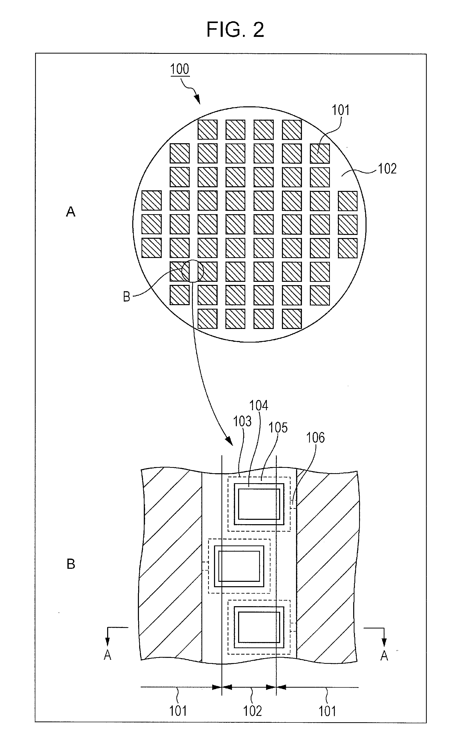
[0176]FIG. 13 illustrates the configuration of the semiconductor wafer. Further, FIG. 14 illustrates the configuration of the semiconductor device.

[0177]The semiconductor wafer 100 illustrated in FIG. 13 is in a state in which the conductor layer formed in the opening portion 104 is removed from the semiconductor wafer of the...

third embodiment

6. Third Embodiment

Semiconductor Device and Semiconductor Wafer

[0209]Next, the third embodiment of the semiconductor device and the semiconductor wafer will be described. The third embodiment is different from the second embodiment only in the configurations of the pad electrode and the external connection terminal and the configuration of the insulating portion formed in the circuit board. Therefore, in the description of the third embodiment, only components different from those in the second embodiment described above will be described and the description regarding the components which are the same as in the second embodiment, among the respective components formed on the circuit forming region will be omitted.

[0210]FIG. 22 illustrates the configuration of a semiconductor wafer of the third embodiment. Further, FIG. 23 illustrates the configuration of a semiconductor device of the third embodiment.

[0211]The semiconductor wafer 100 illustrated in FIG. 22 and the semiconductor waf...


PUM


Abstract

The present technology relates to a semiconductor device, a manufacturing method of a semiconductor device, a semiconductor wafer, and electronic equipment, which allow a semiconductor device, in which miniaturization is possible, to be provided. A semiconductor device includes a semiconductor substrate, a wiring layer that is formed on the semiconductor substrate, and a drive circuit that is provided in a circuit forming region of the semiconductor substrate. Then, the semiconductor device is configured to include a pad electrode that is electrically connected to the drive circuit and exposed from the side surface of the wiring layer, and an external connection terminal that is provided in side surfaces of the semiconductor substrate and the wiring layer, and is electrically connected to the pad electrode.

Description

TECHNICAL FIELD[0001]The present technology relates to a semiconductor device, a manufacturing method of the semiconductor device, a semiconductor wafer in which a semiconductor device is formed, and electronic equipment to which a semiconductor device is applied.BACKGROUND ART[0002]The demand of a solid state imaging device (image sensor) as a semiconductor device used in electronic equipment has been increasing. For the solid state imaging device, a structure of a so-called back-illumination has been proposed in which a drive circuit is formed on the surface of a semiconductor substrate and a back surface is a light receiving side, in order to intend to improve photoelectric conversion efficiency and sensitivity with respect to incident light. In the backside illumination type solid state imaging device, it is possible to increase a light receiving aperture ratio of the light receiving surface, and to increase an incident area of light in the same chip area.[0003]Further, in the b...

Claims


Application Information

Patent Timeline
Patent Type & Authority Patents(United States)
IPC IPC(8): H01L27/146
CPCH01L27/14634H01L27/1464H01L27/1469H01L27/14636H01L27/14689H01L22/14H01L27/0688H01L24/06H01L2224/05554H01L23/481
Inventor KATAOKA, TOYOTAKA
Owner SONY CORP
Why Eureka
Try Eureka