Pixel structure
a pixel structure and pixel technology, applied in the field of pixel structure, can solve the problem of limited viewing angle of liquid crystal display, and achieve the effect of improving the viewing angl
- Summary
- Abstract
- Description
- Claims
- Application Information
AI Technical Summary
Benefits of technology
Problems solved by technology
Method used
Image
Examples
Embodiment Construction
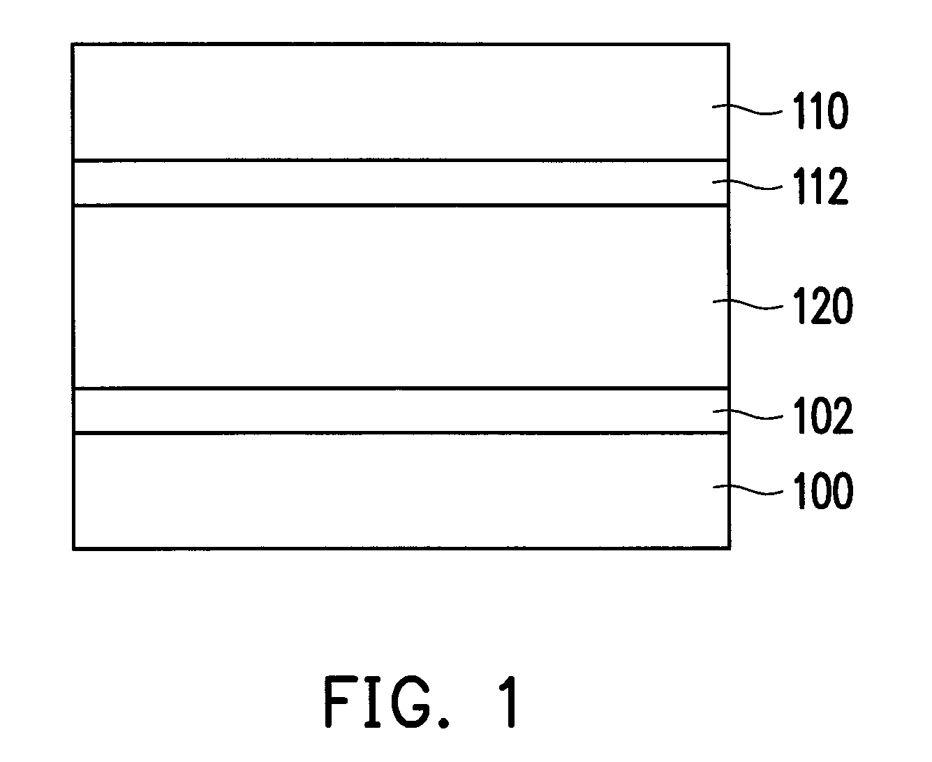
[0023]FIG. 1 is a schematic cross-sectional diagram of a display panel according to an embodiment of the invention.
[0024]Referring to FIG. 1, the display panel of the present embodiment includes a first substrate 100, a second substrate 110, and a display medium 120 disposed between the first substrate 100 and the second substrate 110.
[0025]The first substrate 100 is disposed opposite to the second substrate 110. The material of each of the first substrate 100 and the second substrate 110 can be glass, quartz, an organic polymer, or other suitable materials. The display medium 120 is, for instance, a liquid crystal material. In other words, the display panel of the present embodiment is, for instance, a liquid crystal display panel. However, the invention is not limited thereto. In other embodiments, the display medium 120 can also be other display materials such as an organic light-emitting diode material, an inorganic light-emitting diode material, an electrophoretic display mater...
PUM
| Property | Measurement | Unit |
|---|---|---|
| height H1 | aaaaa | aaaaa |
| height H1 | aaaaa | aaaaa |
| angle | aaaaa | aaaaa |
Abstract
Description
Claims
Application Information


