Method for forming a strained semiconductor structure

a technology of strained semiconductors and buffer layers, applied in the direction of semiconductor devices, basic electric elements, electrical apparatus, etc., can solve the problems of reducing device performance, reducing device stability, and reducing device performance, so as to facilitate the handling improve the stability of the strain relaxed buffer layer, and improve the effect of material quality

Active Publication Date: 2016-03-29
INTERUNIVERSITAIR MICRO ELECTRONICS CENT (IMEC VZW) +1
View PDF4 Cites 0 Cited by
  • Summary
  • Abstract
  • Description
  • Claims
  • Application Information

AI Technical Summary

Benefits of technology

[0008]The disclosure may be based, at least in part, on the realization that prior art methods for fabricating stained semiconductor structures involves challenging processes for removal of oxides from a strain relaxed buffer (SRB) layer comprising, for instance, SiGe or SiC. Removal of oxide from the SRB layer is generally important for efficient and high-yield fabrication of the strained semiconductor structures. The presence of oxides on the SRB layers may lead to variations in the recess being formed. Further, oxide residues on the SRB layer may lead to surface roughness and defects in the strained semiconductor structures being formed on the SRB layer, which in turn may lead to reduced device performance. Oxide removal from surfaces such as SiGe is, moreover, known to be challenging and commonly involves complicated pre-cleaning and high-temperature baking steps. Consequences of the elevated temperatures, typically around 700-800° C., during baking is that roughening of the SiGe surface, Ge-migration, and / or Ge coalescence may occur, which may in turn reduce device performance.
[0031]According to one embodiment of the present disclosure, the SiC material may have a C content in the range 0.01-10%, preferably 0.1-5%. The preferred range of 0.1-5% of C is advantageous as it provides sufficient strain in the strained semiconductor structure and further counteracts dislocation formation in the strained semiconductor structure.

Problems solved by technology

Further, oxide residues on the SRB layer may lead to surface roughness and defects in the strained semiconductor structures being formed on the SRB layer, which in turn may lead to reduced device performance.
Oxide removal from surfaces such as SiGe is, moreover, known to be challenging and commonly involves complicated pre-cleaning and high-temperature baking steps.
Consequences of the elevated temperatures, typically around 700-800° C., during baking is that roughening of the SiGe surface, Ge-migration, and / or Ge coalescence may occur, which may in turn reduce device performance.

Method used


Image

  • Method for forming a strained semiconductor structure
  • Method for forming a strained semiconductor structure
  • Method for forming a strained semiconductor structure

Examples


Embodiment Construction

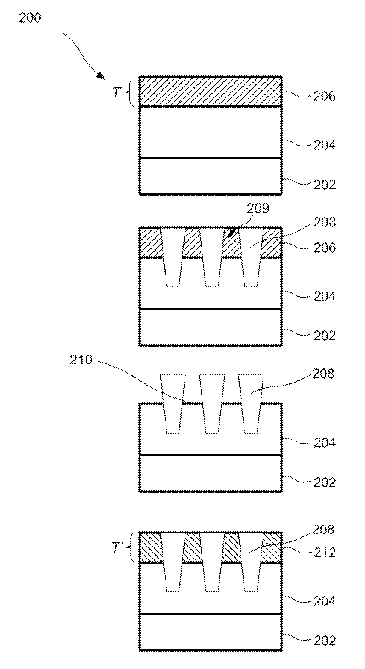
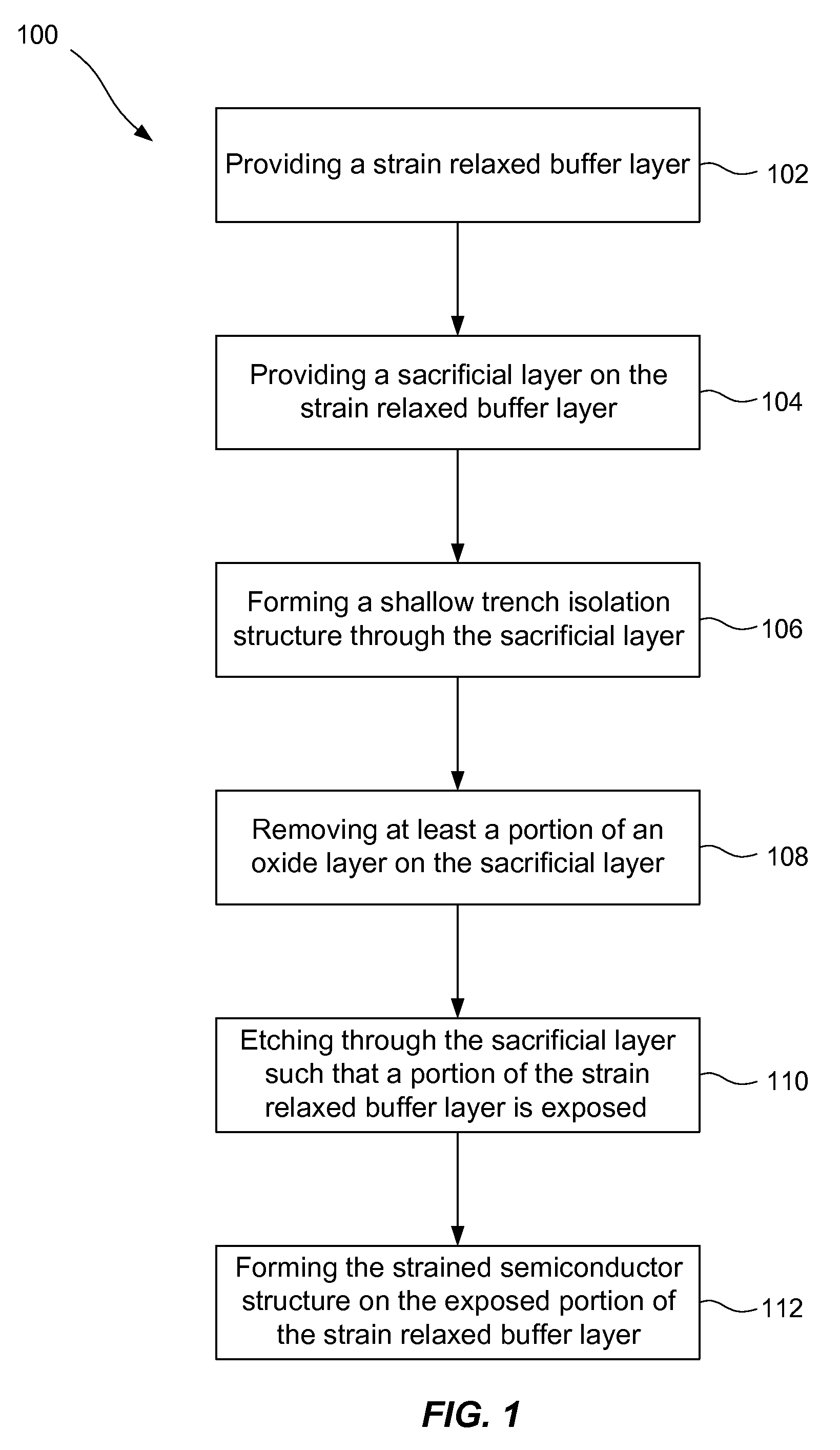
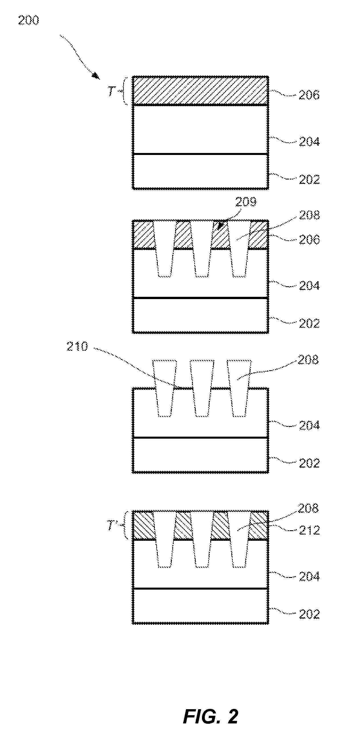
[0037]FIG. 1 illustrates a method 100 for forming a strained semiconductor structure. The method 100 comprises providing a strain relaxed buffer layer 102, providing a sacrificial layer on the strain relaxed buffer layer 104, forming a shallow trench isolation structure through the sacrificial layer 106, removing at least a portion of an oxide layer on the sacrificial layer 108, etching through the sacrificial layer such that a portion of the strain relaxed buffer layer is exposed 110, and forming the strained semiconductor structure on the exposed portion of the strain relaxed buffer layer 112.

[0038]The method 100 is based, at least in part, on the realization that by using a sacrificial layer on the top of the strain relaxed buffer layer (SRB layer) oxide formation and atom migration on the SRB layer may in relation to prior art be counteracted when forming the strained semiconductor structure. The method may therefore provide well-controlled trench recess and improved regrowth of...


PUM


Abstract

The present disclosure relates to a method for forming a strained semiconductor structure. The method comprises providing a strain relaxed buffer layer, forming a sacrificial layer on the strain relaxed buffer layer, forming a shallow trench isolation structure through the sacrificial layer, removing at least a portion of an oxide layer on the sacrificial layer, etching through the sacrificial layer such that a portion of the strain relaxed buffer layer is exposed, forming the strained semiconductor structure on the exposed portion of the strain relaxed buffer layer.

Description

CROSS-REFERENCE TO RELATED APPLICATION[0001]This application claims priority to European Patent Application No. 13173380.0 filed on Jun. 24, 2013, the contents of which are hereby incorporated by reference.FIELD OF THE DISCLOSURE[0002]The present disclosure relates to a method for forming a strained semiconductor structure, the structure being stained in order to improve the performance of the structure.BACKGROUND OF THE DISCLOSURE[0003]There is a continuous demand for improved integrated circuits having higher performance and lower power consumption. Traditionally, the development of integrated circuits has to a large extent been relying on continuous downscaling of semiconductor structures, such as complementary metal oxide semiconductor (CMOS) devices. To push technology to even smaller dimensions, new device technologies, such as Fin Field Effect Transistor (FinFET) structures, have been introduced in the CMOS mainstream starting from the 14 nm node and below. The FinFET technol...

Claims


Application Information

Patent Timeline
Patent Type & Authority Patents(United States)
IPC IPC(8): H01L21/02H01L21/762H01L29/10H01L21/3065
CPCH01L21/02658H01L21/02587H01L21/76224H01L29/1054H01L21/3065H01L21/18H01L21/76
Inventor LEE, SEUNG, HUNWITTERS, LIESBETHLOO, ROGER
Owner INTERUNIVERSITAIR MICRO ELECTRONICS CENT (IMEC VZW)
Why Eureka
Try Eureka