Method of forming an interconnect structure with high process margins

a technology of interconnect structure and process margin, which is applied in the direction of semiconductor devices, electrical equipment, semiconductor/solid-state device details, etc., can solve the problems of increasing the risk of short-circuiting, increasing the difficulty of deep tungsten contact formation, and increasing the difficulty of alignment of via parts and line parts, so as to reduce the aspect ratio of copper metallization, improve the reliability of tungsten, and reduce the effect of device performan

Active Publication Date: 2015-07-23
NAN YA TECH
View PDF5 Cites 10 Cited by
  • Summary
  • Abstract
  • Description
  • Claims
  • Application Information

AI Technical Summary

Benefits of technology

[0006]In comparison with an all-copper dual damascene, there are a few advantages when utilizing the present invention. The all-copper dual damascene includes via parts and line parts, and both are filled with copper. It can become very challenging for conventional Cu-based processing since a PVD barrier and seed layers are typically needed, which may not have sufficient step coverage inside deep, high aspect ratio vias and also suffers from a phenomenon called “bread loafing” near the opening of the trench, thus leading to copper void formation. The present invention resolves this challenge for copper deposition by filling the plurality of via holes with tungsten and applying a first mask layer, thereby reducing the aspect ratio of the copper metallization that needs to be filled. Due to high aspect ratio holes, the contact structures below the copper interconnects may develop keyholes, which are common in deep contacts. When copper interconnects are directly formed on top of deep contacts with keyholes, copper atoms may penetrate through the contacts and degrade the device performance or suffer from reliability loss. The present invention resolves this issue since it has more reliable tungsten via part separating the copper interconnects from the deep contacts in the substrate that are prone to keyhole formation.
[0007]The present invention provides an interconnect structure and the method for preparing the same. It is important for the Cu-based BEOL stacks to make electrical connections to the high aspect ratio tungsten contacts in the FEOL processes. The present invention provides a higher aligning margin for the connections of via parts and line parts. The risk of short-circuiting may be decreased and the process margin may be increased. The method for forming the interconnect structure comprises the steps of: forming a first mask layer with a plurality of first openings over the first insulating layer; forming a second insulating layer over the mask layer; forming a second mask layer with a plurality of second openings over the second insulating layer; performing an etching process by using the second mask layer to form a plurality of cavities penetrating through the second insulating layer, the first mask layer, and the first insulating layer; and filling the plurality of cavities with at least one conductive material.
[0008]The advantage of the present invention is that of having one less critical alignment step than the conventional dual damascene since the plurality of via holes are self-aligned to the plurality of trenches, which serve as a conducting wire.
[0009]The present invention provides some economical benefits such as having only one dielectric etch process as opposed to the conventional dual damascene which requires two dielectric etching processes for the via and the trenches, and the present invention does not require a WCMP process, which has a high cost and brings about dishing and erosion. Furthermore, the present invention is able to block penetrating copper atoms by filling the plurality of via holes with tungsten and applying a first mask layer. As such, the present invention does not need copper barrier layers or copper seed layers to deposit into deep and high aspect ratio vias. In addition, since the present invention has reliable electric performance, it is able to prevent copper voids from forming in the interconnect since the plurality of via holes are already filled with a first conductive material.
[0010]The foregoing has outlined rather broadly the features and technical advantages of the present disclosure in order that the detailed description of the disclosure that follows may be better understood. Additional features and advantages of the disclosure will be described hereinafter, which form the subject of the claims of the disclosure. It should be appreciated by those skilled in the art that the conception and specific embodiment disclosed may be readily utilized as a basis for modifying or designing other structures or processes for carrying out the same purposes of the present disclosure. It should also be realized by those skilled in the art that such equivalent constructions do not depart from the spirit and scope of the disclosure as set forth in the appended claims.

Problems solved by technology

As devices continue to minimize, the formation of the deep tungsten contacts becomes more and more difficult because of poor etch profiles and a high risk of under etching.
Moreover, the alignment margin between the tight pitched copper line and the tungsten via continues to get smaller, and thus causes a higher risk of short-circuiting.
Since the conventional dual damascene comprises such parts and processes, the alignment of the via parts and line parts becomes increasingly difficult due to the minimization of devices.
In FIGS. 5 and 6, an etching back process for removing a first conductive material on an upper surface of a second insulating layer is performed rather than a tungsten CMP (WCMP) process, which has a high cost and brings about dishing and erosion.
Additionally, the line height of the conventional dual damascene is not easy to control in the two dielectric etching processes.
It can become very challenging for conventional Cu-based processing since a PVD barrier and seed layers are typically needed, which may not have sufficient step coverage inside deep, high aspect ratio vias and also suffers from a phenomenon called “bread loafing” near the opening of the trench, thus leading to copper void formation.
When copper interconnects are directly formed on top of deep contacts with keyholes, copper atoms may penetrate through the contacts and degrade the device performance or suffer from reliability loss.

Method used


Image

  • Method of forming an interconnect structure with high process margins
  • Method of forming an interconnect structure with high process margins
  • Method of forming an interconnect structure with high process margins

Examples


Embodiment Construction

[0019]The following description of the disclosure accompanies drawings, which are incorporated in and constitute a part of this specification, and illustrate embodiments of the disclosure, but the disclosure is not limited to the embodiments. In addition, the following embodiments can be properly integrated to complete another embodiment.

[0020]The present disclosure is directed to a method of forming reliable contacts with a high process margin. In order to make the present disclosure completely comprehensible, detailed steps and structures are provided in the following description.

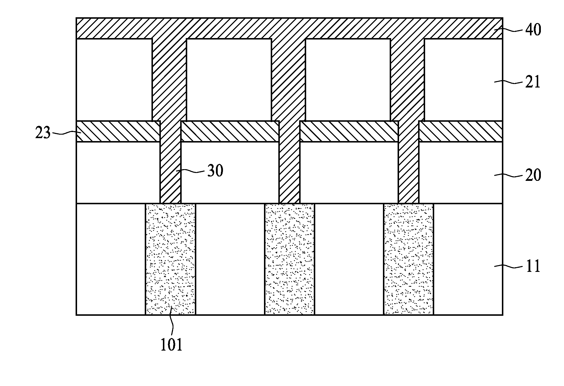
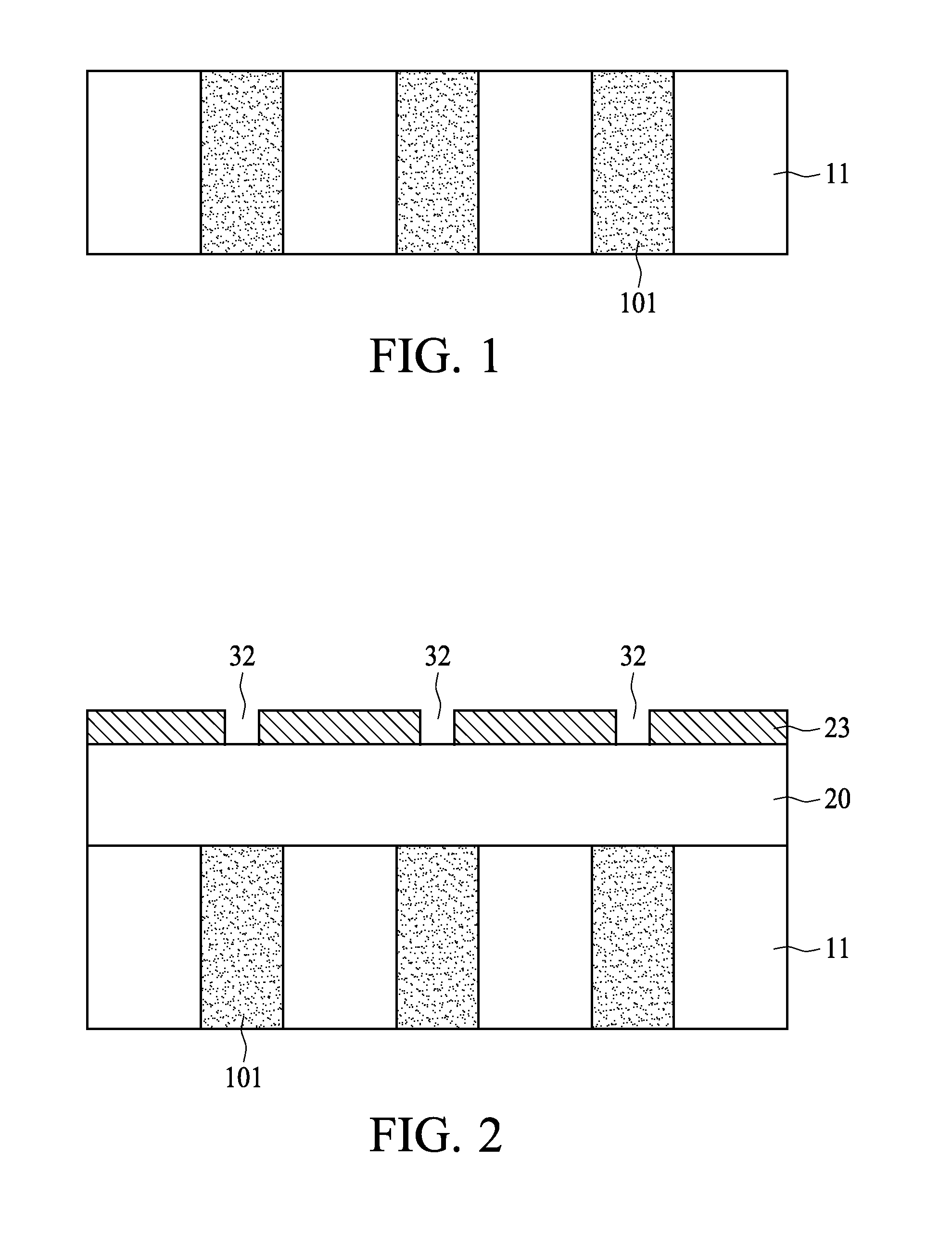
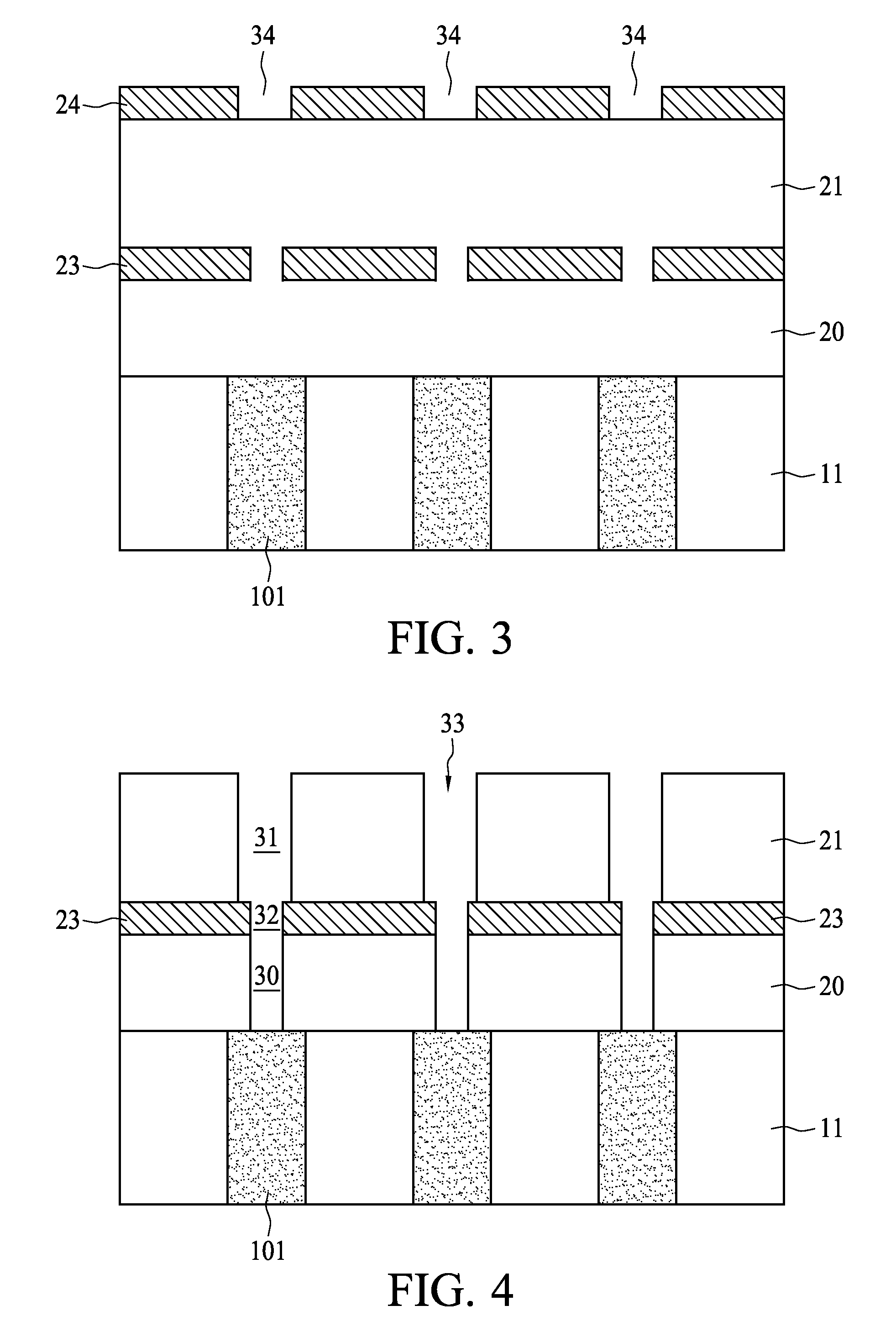
[0021]FIG. 1 is a substrate 11 with a plurality of contacts 101. Under the plurality of contacts 101, there may be a plurality of devices or MOSFETs electrically connected with the plurality of contacts 101. The plurality of contacts 101 are filled with metal, for example, tungsten. The tungsten contact holes are formed by front-end-of-line processing, and upper parts of the substrate 11 are further plana...


PUM


Abstract

A method of forming an interconnect structure with high process margin. The present invention provides higher aligning margin for the connection of via parts and line parts. The method for forming the interconnect structure includes the steps of: forming a first mask layer with a plurality of first openings over the first insulating layer; forming a second insulating layer over the mask layer; forming a second mask layer with a plurality of second openings over the second insulating layer; performing an etching process by using the second mask layer to form a plurality of cavities penetrating through the second insulating layer, the first mask layer, and the first insulating layer; and filling the plurality of cavities with at least one conductive material.

Description

BACKGROUND[0001]1. Technical Field[0002]The present disclosure relates to an interconnect structure and the method for preparing the same. More particularly, the invention is related to an interconnect structure and the method for preparing the same with high process margins.[0003]2. Description of Related Arts[0004]It is a common requirement for Cu-based back-end-of-line (BEOL) stacks to make electrical connections with high aspect ratio tungsten contacts in front-end-of-line (FEOL) processes. As semiconductor devices are made, the interconnection electrically links the devices and conductive line parts together. There are via parts and line parts that form an interconnected structure. The via parts are usually filled with tungsten and the method of deposition is highly developed. The line parts are usually filled with copper, which has high conductivity, low resistance, and is able to prevent electron migration. As devices continue to minimize, the formation of the deep tungsten c...

Claims


Application Information

Patent Timeline
Patent Type & Authority Applications(United States)
IPC IPC(8): H01L23/522H01L21/768
CPCH01L23/5226H01L21/76877H01L21/76897H01L2924/0002H01L23/53295H01L23/53228H01L23/53257H01L21/7681H01L2924/00
Inventor BIAN, ZAI LONG
Owner NAN YA TECH
Why Eureka
Try Eureka