Method of manufacturing substrate having cavity

a manufacturing method and substrate technology, applied in the direction of printed element electric connection formation, association of printed circuit non-printed electric components, coatings, etc., can solve the problems of tendency for variation, cracking in the bottom surface, and difficulty in creating a cavity with smooth so as to maintain the smoothness of inner walls and bottom surfaces

Active Publication Date: 2016-03-29
TAIYO YUDEN KK
View PDF11 Cites 6 Cited by
  • Summary
  • Abstract
  • Description
  • Claims
  • Application Information

AI Technical Summary

Benefits of technology

[0010]An object of the present invention is to provide a method of manufacturing a substrate having a cavity that is not susceptible to variation in cross-sectional dimensions and depth of the cavity while maintaining smoothness of the inner walls and bottom surface.
[0013]According to the present invention, it is possible to provide a method of manufacturing a substrate having a cavity that is not susceptible to variation in cross-sectional dimensions and depth thereof while maintaining smoothness of the bottom surface.

Problems solved by technology

However, if the cavity is formed such that the thickness below the bottom surface is very thin (100 μm or less, for example) then there is a risk that stress resulting from cutting will result in damage such as cracking in the bottom surface.
Also, cutting involves a dimensional tolerance of at least ±tens of μm, and thus, there is a tendency for variation to occur in the cross-sectional dimensions and depth of the cavity, and it is difficult to create a cavity with smooth inner walls and bottom surface.
However, if the material to be etched is synthetic resin, the time taken to etch is generally longer than if the material were metal.
Also, the etchant used for the synthetic resin generally depends on the type of synthetic resin, but this method is unrealistic due to some types of resins (such as epoxy resin) requiring dangerous substances such as concentrated sulfuric acid or chromic acid.
However, it is difficult for the cross-sectional dimensions of the penetrating holes formed in the respective layers to match perfectly, and it is difficult to stack the respective layers such that the penetrating holes align without being offset, and thus variation tends to occur in the cross-sectional dimensions of the cavity, which makes it difficult to have a cavity with smooth inner walls.
Also, if an adhesive is used when stacking the respective layers, there is a risk that some of the adhesive seeps out to the bottom surface of the cavity when the layers are stacked, which results in variation in depth of the cavity or loss of smoothness in the bottom surface.

Method used


Image

  • Method of manufacturing substrate having cavity
  • Method of manufacturing substrate having cavity
  • Method of manufacturing substrate having cavity

Examples


modification examples

of Second Manufacturing Method

[0089]Below, modification examples of the second manufacturing method described above will be described.

modification example 1

[0090]In the second manufacturing method, a step was used in which the adhesive sheet 33 is bonded on the bottom surfaces of the signal wiring lines 32a and the cylindrical via 32b (refer to FIG. 17), but as shown in FIG. 23, instead of using the adhesive sheet 33, a sheet-shaped material made of a material for the insulating layer 37 that has not yet been cured may be bonded to the bottom surfaces of the signal wiring lines 32a and the cylindrical via 32b, with the bottom surface of the dummy part 34 inserted into the penetrating hole 31a being bonded to the sheet-shaped material and the sheet-shaped material then being cured by heat treatment. In this manner, it is possible to omit the aforementioned step.

modification example 2

[0091]In the second manufacturing method, a step was used in which the sheet-shaped material made of the material for the insulating layer 35 and the insulating portion 36 that has not yet been cured is bonded to the top surface of the base layer 31, and then the sheet-shaped material is pressed towards the base layer 31 such that a portion thereof fills the ring-shaped gap between the inner wall of the penetrating hole 31a and the outer wall of the dummy part 34 and into the inner hole of the cylindrical via 32b with remaining portions being left remaining in a layer shape on the bottom surface and the top surface of the base layer 31 (refer to FIG. 17). However, as shown in FIG. 24, a step may be taken in which a sheet-shaped material made of the material for the insulating layer 37 that has not yet been cured is bonded onto the bottom surfaces of the signal wiring lines 32a and the cylindrical via 32b and the bottom surface of the dummy part 34 inserted into the penetrating hole ...


PUM


Abstract

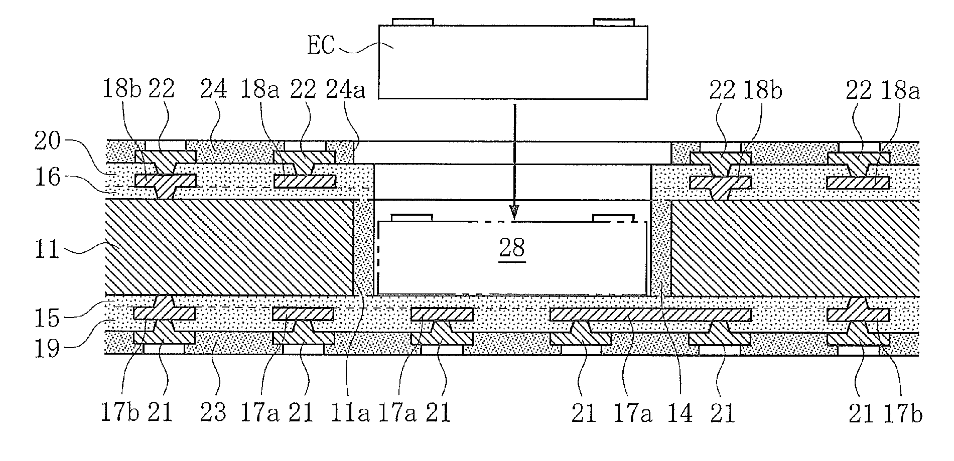
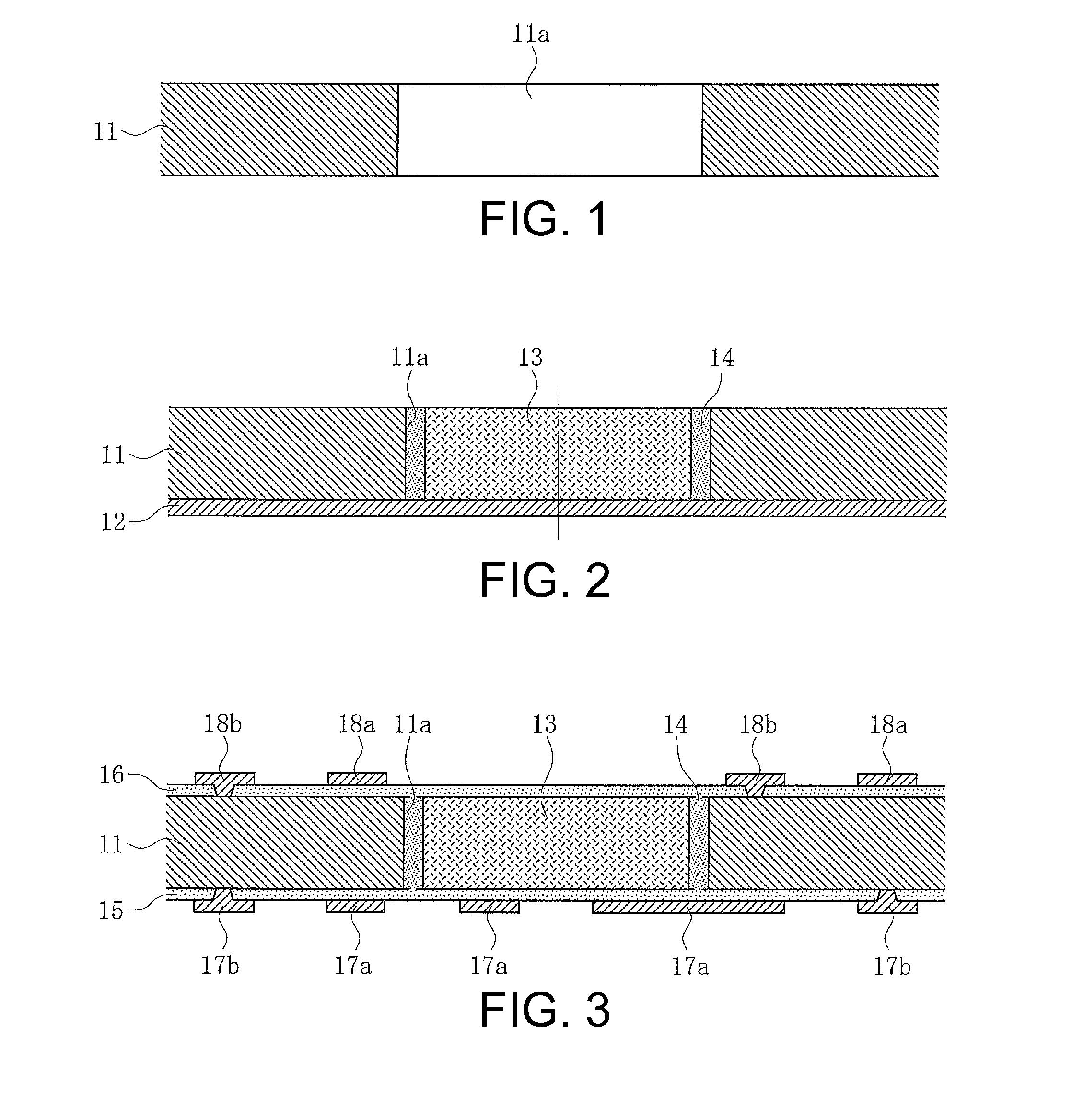
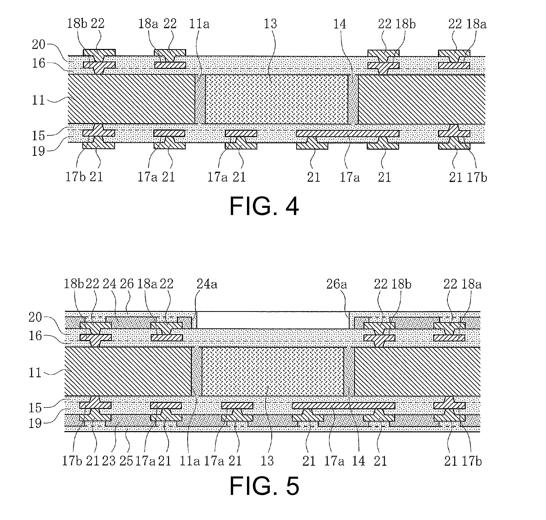
The method of manufacturing a substrate includes: forming a penetrating hole in a base layer; inserting a metal dummy part in the penetrating hole; forming an insulating portion made of synthetic resin to fill a ring-shaped gap between the penetrating hole and the dummy part; forming lower insulating layers, covering the bottom surface of the dummy part, that are made of synthetic resin on the bottom surface of the base layer to be continuous with the insulating portion; forming upper insulating layers, covering the top surface of the dummy part, that are made of synthetic resin on the top surface of the base layer to be continuous with the insulating portion; forming an exposing hole by routing in the upper insulating layers to expose the top surface of the dummy part; and forming a cavity by removing the dummy part exposed through the exposing hole by etching.

Description

BACKGROUND OF THE INVENTION[0001]1. Field of the Invention[0002]The present invention relates to a method of manufacturing a substrate having a cavity (recess) for installing an electronic component therein.[0003]2. Description of Related Art[0004]With mobile devices such as mobile phones and smartphones having a smaller profile, there is strong demand for reducing the thickness of the substrate having an electronic component installed therein, and one method of realizing reduced thickness is to provide a cavity (recess) (refer to Patent Document 1 below, for example). That is, by installing an electronic component inside the cavity, it is possible to reduce the thickness of the substrate having installed therein the electronic component.[0005]Examples of methods to provide the substrate with a cavity include: (M1) forming a cavity by mechanical cutting; (M2) forming a cavity by chemical etching; and (M3) forming a cavity by stacking a plurality of layers having penetrating holes al...

Claims


Application Information

Patent Timeline
Patent Type & Authority Patents(United States)
IPC IPC(8): B05D5/12H05K3/46H05K1/18H05K3/06H05K3/44B05D3/12H05K3/00H05K3/04H05K3/30H05K3/42
CPCH05K3/4697H05K3/4647B05D3/12B05D5/12H05K1/185H05K3/007H05K3/0044H05K3/0094H05K3/04H05K3/06H05K3/30H05K3/42H05K3/445H05K3/4608H05K2201/10204
Inventor MIYAZAKI, MASASHISUGIYAMA, YUICHISAWATARI, TATSUROYOKOTA, HIDEKIHATA, YUTAKA
Owner TAIYO YUDEN KK
Why Eureka
Try Eureka