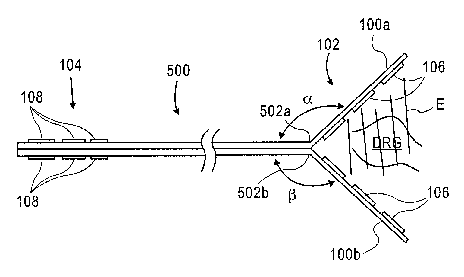
[0014]The present invention provides devices, systems and methods for stimulation of tissues and structures within a body of a patient. In particular, implantable leads are provided which are flexible, reliable and easily manufacturable for a variety of medical applications. Such leads are particularly suitable for stimulation of the spinal anatomy, more particularly suitable for stimulation of specific nerve anatomies, such as the dorsal root (optionally including the dorsal root ganglion). Such specificity is enhanced by the design attributes of the leads.
[0015]The implantable leads of the present invention utilize a flexible circuit. Typically, the flexible circuit includes an array of conductors bonded to a thin dielectric film. Example dielectric films include polyimide, polyvinylidene fluoride (PVDF) or other biocompatible materials to name a few. The conductors are comprised of biocompatible conductive metal(s) and / or alloy(s), such as gold, titanium, tungsten, titanium tungsten, titanium nitride, platinum, iridium, or platinum-iridium alloy, which is plated onto the dielectric film. The base and metal construct is then etched to form a circuit (i.e. an electrode pad contact and a “trace” to connect the pad to a connector). In some embodiments, redundancy in the “traces” is provided by utilizing multiple traces to the same content to improve reliability.
[0016]Some advantages of leads comprised of a flexible circuit over traditional leads are greater reliability, size and weight reduction, elimination of mechanical connectors, elimination of wiring errors, increased impedance control and signal quality, circuit simplification, greater operating temperature range, and higher circuit density. In addition, lower cost is another advantage of using flexible circuits. In some embodiments, the entire lead will be formed from a flexible circuit. Also, in some embodiments, the lead will include an integrated connector for connection to an electronics package.
[0017]One main advantage of the flexible circuitry lead is its thinness and therefore flexibility. The thickness of the dielectric film typically ranges from 7.5 to 125 μm (0.3 to 5 mils). However, in some embodiments, the lead will be comprised of a flexible circuit having a base layer of 0.5 to 2 mils thick.
[0020]In some embodiments, the flexible circuit is created with methods of the present invention. For example, metal deposition, such as vapor deposition, sputtering techniques or plasma fields, is used to coat the film structure with metal to form the electrodes and traces. In such embodiments, the film structure is comprised of polyvinylidene fluoride (PVDF). The process may utilize PVDF in either sheet form or, preferably, in roll form, with cooling to reduce thermal stresses between the dielectric film structure and the metal coat. The PVDF is coated with an adhesion layer, such as titanium or titanium-tungsten alloy, which will improve the reliability of the bond between the dielectric film structure and the electrodes and traces that will be deposited thereon. The adhesion layer is then coated, such as sputter coated, with a seed layer of conductive biocompatible metal, such as gold or platinum. After such metallization, the seed layer is patterned, either by photolithography and wet etch, or by laser ablation to form the shapes of the traces and electrodes. After patterning the seed layer of metal, sputtering or electroplating is used to increase the thickness of the traces in order to improve conductivity, and then again to create the final electrode working surface. Possible trace materials include platinum, gold, iridium-oxide, a combination thereof or any other conductive biocompatible metal suitable for implantation. The electrode surface may be coated over the entire metallization of the lead, or selectively and only over the intended electrode surface with an inert metal such as platinum, iridium-oxide, or combination thereof. In some embodiments, the adhesion layer of titanium or titanium-tungsten alloy is sputter coated with a seed layer of gold, then sputter coated with platinum and then electroplated with platinum. In other embodiments, the adhesion layer of titanium or titanium-tungsten alloy is sputter coated with a seed layer of gold, then electroplated with gold and then electroplated with platinum. In yet other embodiments, the adhesion layer of titanium or titanium-tungsten alloy is sputter coated with a seed layer of platinum, then electroplated with platinum. It may be appreciated that other combinations may also be used.

