

Semiconductor device and method for fabricating the same
a semiconductor and device technology, applied in the direction of semiconductor devices, electrical devices, transistors, etc., can solve the problem that the device strain cannot be significantly increased
- Summary
- Abstract
- Description
- Claims
- Application Information
AI Technical Summary
Benefits of technology
Problems solved by technology
Method used
Image

Examples
Embodiment Construction
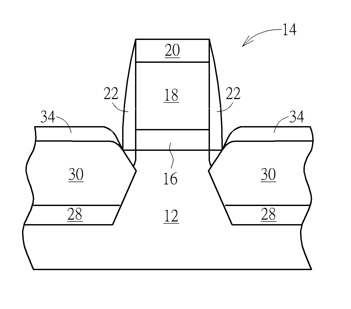
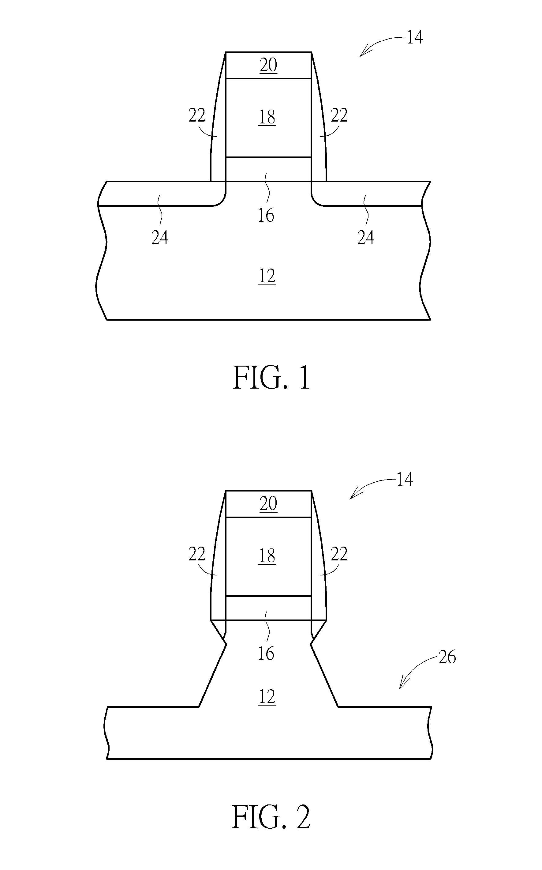
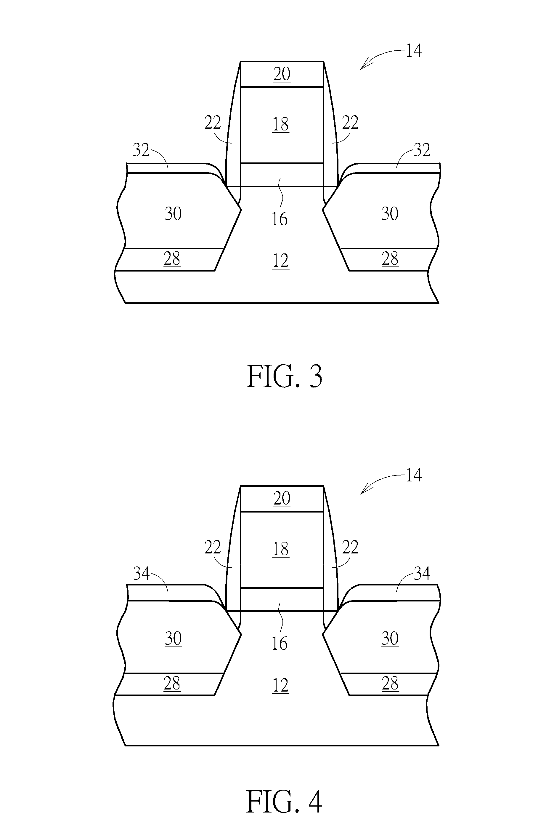
[0010]Referring to FIGS. 1-4, FIGS. 1-4 illustrate a method for fabricating semiconductor device according to a preferred embodiment of the present invention. As shown in FIG. 1, a substrate 12 is first provided, and at least one gate structure 14 is formed on the substrate 12. In this embodiment, the formation of the gate structure 14 could be accomplished by sequentially forming a gate dielectric layer, a gate material layer, and a hard mask on the substrate 12, conducting a pattern transfer process by using a patterned resist (not shown) as mask to partially remove the hard mask, gate material layer, and gate dielectric layer through single or multiple etching processes, and stripping the patterned resist for forming a gate structure 14 on the substrate 12. Preferably, the gate structure 14 is composed of a patterned gate dielectric layer 16, a patterned gate material layer 18, and a patterned hard mask 20 and despite only a single gate structure 14 is disclosed in this embodimen...
PUM
 Abstract
Description
Claims
Application Information