Mesoscopic optoelectronic devices comprising arrays of semiconductor pillars deposited from a suspension and production method thereof

a technology of mesoscopic optoelectronic devices and semiconductor pillars, which is applied in the direction of light-sensitive devices, solid-state devices, electrolytic capacitors, etc., can solve the problems of not being able to achieve the effect of consuming and/or requiring too much space/area with the present devices, and achieve the effect of enhancing efficiency and functionality of mesoscopic optoelectronic devices and low cos

Active Publication Date: 2016-05-17
FACULDADE DE CIENCIAS E TECHA DA UNIV NOVA DE LISBOA
View PDF28 Cites 1 Cited by
  • Summary
  • Abstract
  • Description
  • Claims
  • Application Information

AI Technical Summary

Benefits of technology

[0003]The present invention concerns a new fabrication process able to enhance efficiency and functionality of mesoscopic optoelectronic devices. The invented method allows fabricating low cost, efficient, rigid or flexible mesoscopic optoelectronic devices such as photovoltaic solar cells or photo sensors consisting of three-dimensional (3D) arrays of semiconductors micro- or nano-pillars deposited from suspensions of inorganic, organic and hybrid materials using inkjet printing.
[0004]The mesoscopic devices of the present invention employ 3D structures which additionally increase the surface area of the device composed of an interpenetrating network of inorganic, organic or hybrid semiconductor particles of mesoscopic (2-50 nm) size forming junctions. This method allows to further increase of already very high contact area of mesoscopic photovoltaic devices instead of the flat morphology used by conventional thin-film technologies, commonly referred as ‘bulk’ junction devices due to their porous and light structure.

Problems solved by technology

With this invention it is possible to manufacture devices, either as solar cells or photodetectors, among other optoelectronic devices, to be directly applied to power systems such as wind-screens and automobile windows or visors without need of large implanted areas, which is not possible to achieve with the present devices that take and or require too much space / area when the power required is significantly high due to the limitations imposed by the available areas.

Method used


Image

  • Mesoscopic optoelectronic devices comprising arrays of semiconductor pillars deposited from a suspension and production method thereof
  • Mesoscopic optoelectronic devices comprising arrays of semiconductor pillars deposited from a suspension and production method thereof
  • Mesoscopic optoelectronic devices comprising arrays of semiconductor pillars deposited from a suspension and production method thereof

Examples


Embodiment Construction

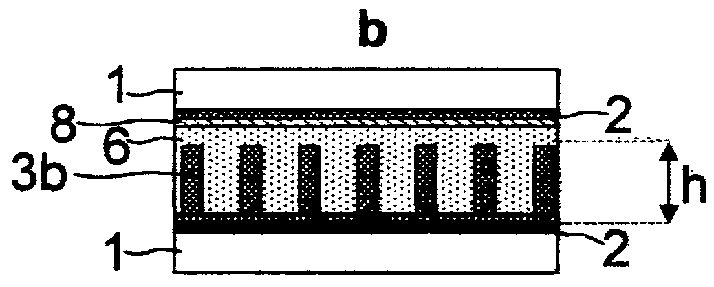
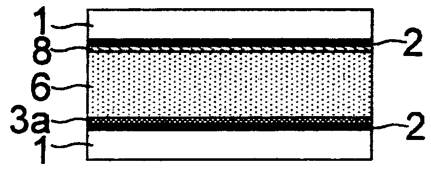
[0070]As previously mentioned, the present invention relates to the method and manufacture process of mesoscopic optoelectronic devices such as solar cells and photo-sensors wherein the active area is significantly enhanced resulting in a increasing the energy conversion efficiency of the light to electrical energy preferably using two possible structures: planar or lateral structures based in micro- or nano-pillars deposited form suspension via Inkjet Printing Technology.

[0071]The present invention will be further described (see FIGS. 1 to 4) illustrating, the development of mesoscopic optoelectronic devices such as solar cells and photosensors using micro- or nano-patterning via preferentially Inkjet Printing Technology.

[0072]The following embodiments help to describe inventive aspects of the invention, not necessarily finished devices, and are therefore able to be combined and partially used as appropriate.

[0073]As depicted in FIGS. 1 and 3, the layered (planar) structure device ...


PUM


Abstract

The invention illustrates an innovative way to fabricate low cost, efficient, rigid or flexible mesoscopic optoelectronic devices such as photovoltaic (PV) solar cells or photo sensors (b) comprising three-dimensional arrays of semi-conductive micro- or nano-pillars (3b) deposited from suspensions e.g. by inkjet printing. Said pillars additionally increase the surface area of the device composed of an interpenetrating network of semiconductor particles of mesoscopic (2-50 nm) size forming junctions. In the present invention the active surface area is significantly increased when compared to previous flat structures (a, 3a), being fabricated preferably by inkjet patterning. Additionally, the invention allows for production of much more functional devices when compared with conventional mesoscopic PV cells due to smaller structure density what makes the layer more resistive to mechanical failure when bending. The invention also describes the device substrate (1), contact and electrode (2, 8), ion conductor (6) and fabrication parameters (h, d).

Description

CROSS-REFERENCE TO RELATED APPLICATIONS[0001]This application is a §371 national stage of PCT International Application No. PCT / PT2010 / 000057, filed Dec. 9, 2010, the contents of which are hereby incorporated by reference in its entirety.TECHNICAL FIELD[0002]The present invention concerns a new fabrication process able to enhance efficiency and functionality of mesoscopic optoelectronic devices. The invented method allows fabricating low cost, efficient, rigid or flexible mesoscopic optoelectronic devices such as photovoltaic solar cells or photo sensors comprising of three-dimensional (3D) arrays of semiconductors micro- or nano-pillars deposited from suspensions of inorganic, organic and hybrid materials preferably using inkjet printing.SUMMARY OF THE INVENTION[0003]The present invention concerns a new fabrication process able to enhance efficiency and functionality of mesoscopic optoelectronic devices. The invented method allows fabricating low cost, efficient, rigid or flexible ...

Claims


Application Information

Patent Timeline
Patent Type & Authority Patents(United States)
IPC IPC(8): H01L51/42B82Y40/00H01L51/00H01L31/18H01G9/20B82Y20/00H01L31/0236
CPCB82Y40/00H01G9/2031H01L51/0005B82Y20/00H01L31/02366H01L31/18Y02E10/542Y02E10/549H10K71/135
Inventor FERRAO DE PAIVA MARTINS, RODRIGOCORREIA FORTUNATO, ELVIRA MARIAJERZY WOJCIK, PAWEL
Owner FACULDADE DE CIENCIAS E TECHA DA UNIV NOVA DE LISBOA
Why Eureka
Try Eureka