Organic electroluminescence display device having a conductive organic layer in contact with an upper electrode

a technology of organic layer and display device, which is applied in the direction of discharge tube luminescnet screen, solid-state device, semiconductor device, etc., can solve the problems of difficult to eliminate luminance unevenness and complicated manufacturing process, and achieves low cathode resistance, eliminate luminance unevenness, and complex manufacturing process

Active Publication Date: 2016-06-07
JAPAN DISPLAY INC
View PDF17 Cites 9 Cited by
  • Summary
  • Abstract
  • Description
  • Claims
  • Application Information

AI Technical Summary

Benefits of technology

[0008]It is considered that the above-described organic EL display devices are effective for achieving the low resistance of the cathode. However, the manufacturing process is complicated, and it is difficult to eliminate the unevenness of luminance between the edge portion of the display area and the central portion of the display area.
[0009]The invention has been made in view of the circumstances described above, and it is an object of the invention to provide an organic EL display device in which the low resistance of an upper electrode formed on the whole surface of a display area is achieved without complicating the manufacturing process.

Problems solved by technology

However, the manufacturing process is complicated, and it is difficult to eliminate the unevenness of luminance between the edge portion of the display area and the central portion of the display area.

Method used


Image

  • Organic electroluminescence display device having a conductive organic layer in contact with an upper electrode
  • Organic electroluminescence display device having a conductive organic layer in contact with an upper electrode
  • Organic electroluminescence display device having a conductive organic layer in contact with an upper electrode

Examples


Embodiment Construction

[0031]Hereinafter, an embodiment of the invention will be described with reference to the drawings. In the drawings, the same or equivalent elements are denoted by the same reference numerals and signs, and a redundant description is omitted.

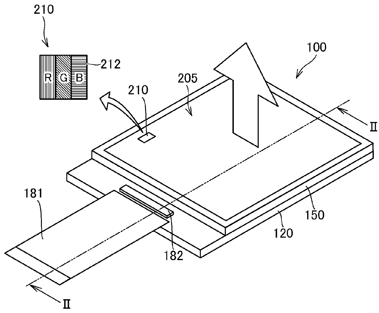
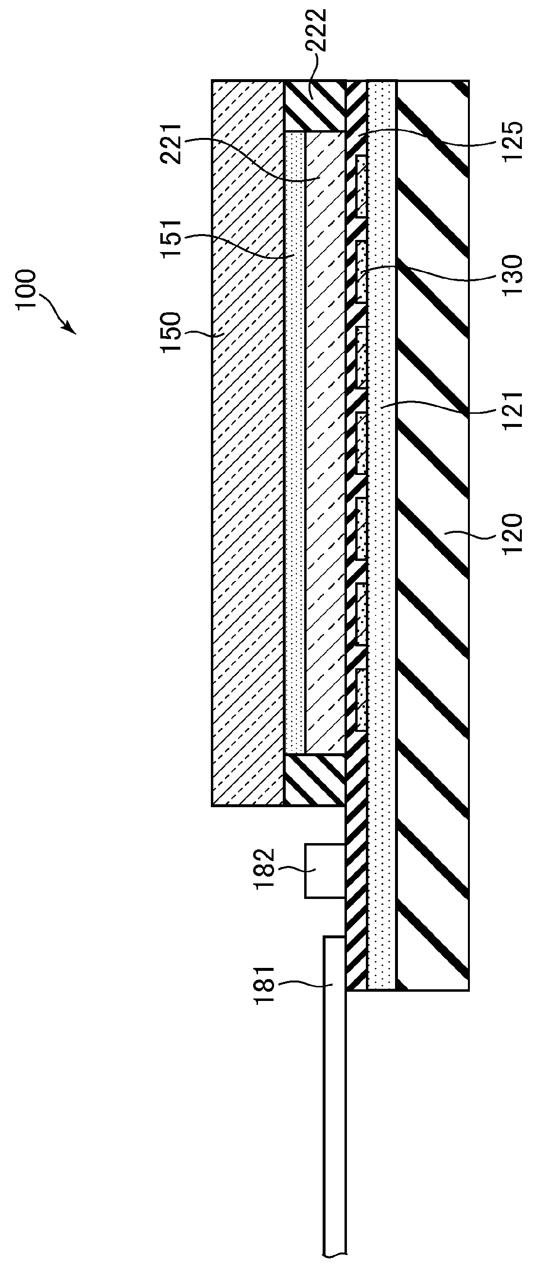
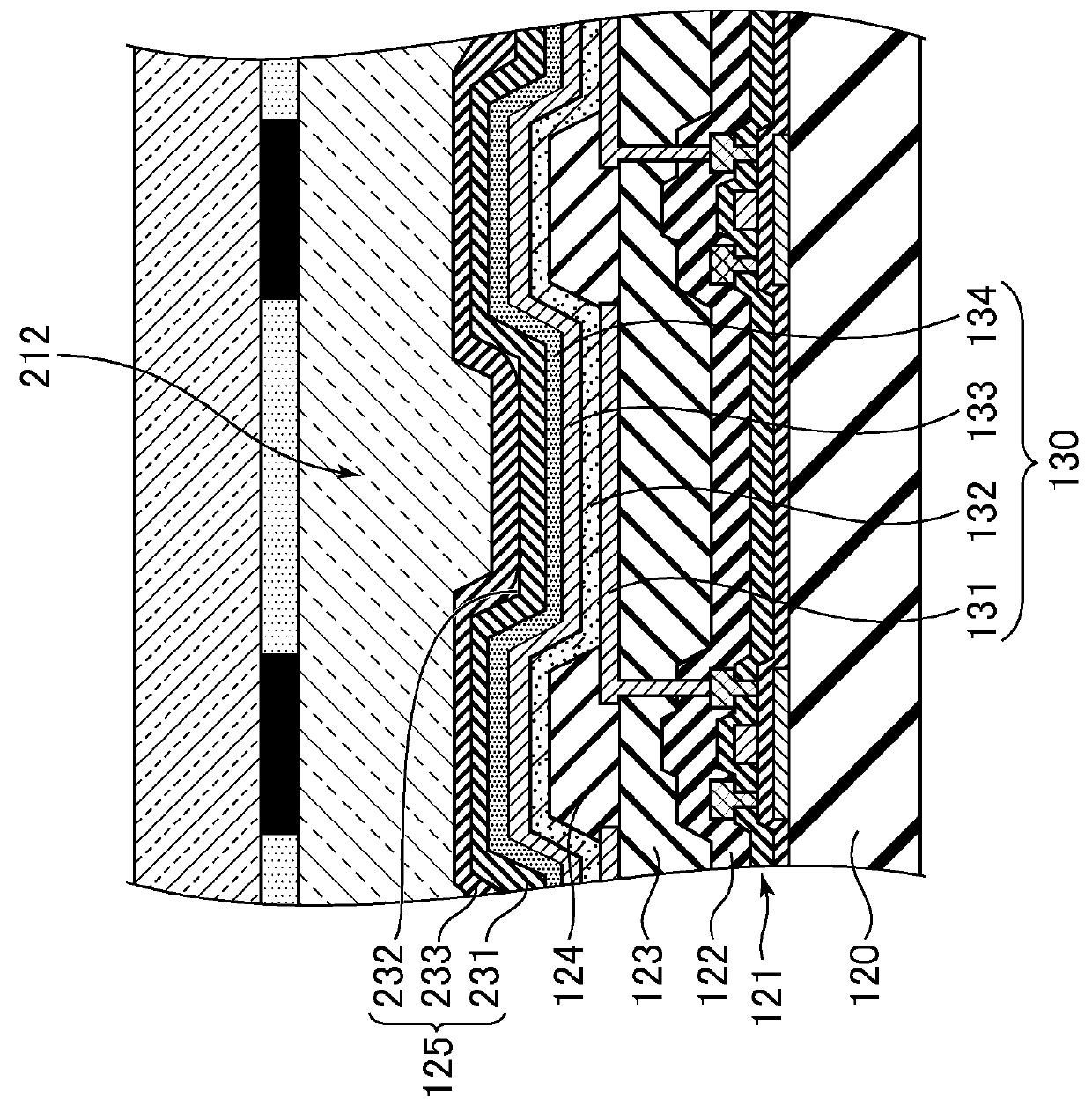
[0032]FIG. 1 schematically shows an organic electroluminescence display device 100 according to the embodiment of the invention. As shown in the drawing, the organic electroluminescence display device 100 includes two substrates, a TFT (Thin Film Transistor) substrate 120 and a counter substrate 150, between which a transparent resin filler 221 (refer to FIG. 2) is sealed. A display area 205 composed of pixels 210 arranged in a matrix is formed in the TFT substrate 120 and the counter substrate 150 of the organic electroluminescence display device 100. The pixel 210 is composed of three sub-pixels 212 from which lights corresponding to three colors of R (red), G (green), and B (blue) are emitted.

[0033]A driver IC (Integrated Circuit) 182 as a dr...


PUM


Abstract

An organic electroluminescence display device includes: a lower electrode that is made of a conductive inorganic material and formed in each of pixels arranged in a matrix in a display area; a light-emitting organic layer that is in contact with the lower electrode and made of a plurality of different organic material layers including a light-emitting layer emitting light; an upper electrode that is in contact with the light-emitting organic layer, formed so as to cover the whole of the display area, and made of a conductive inorganic material; and a conductive organic layer that is in contact with the upper electrode, formed so as to cover the whole of the display area, and made of a conductive organic material.

Description

CROSS-REFERENCE TO RELATED APPLICATION[0001]The present application claims priority from Japanese application JP 2013-206170 filed on Oct. 1, 2013, the content of which is hereby incorporated by reference into this application.BACKGROUND OF THE INVENTION[0002]1. Field of the Invention[0003]The present invention relates to an organic electroluminescence display device.[0004]2. Description of the Related Art[0005]In recent years, image display devices (hereinafter referred to as “organic EL (Electro-Luminescence) display devices”) using a self-luminous body called an organic light-emitting diode (OLED) have been put to practical use. Since the self-luminous body is used, the organic EL display devices are superior in terms of visibility and response speed, compared to a related-art liquid crystal display device, and in addition, a further reduction in thickness is possible because an auxiliary lighting device such as a backlight is not necessary.[0006]In a so-called top-emission displ...

Claims


Application Information

Patent Timeline
Patent Type & Authority Patents(United States)
IPC IPC(8): H01J1/62H01L51/52H01L27/32H01L51/50
CPCH01L51/5234H01L27/3211H01L51/5044H01L51/5253H10K59/35H10K50/131H10K50/828H10K50/844H10K59/351H10K59/124H10K59/121H10K50/82H10K50/822H10K50/8426H10K50/8445H10K2102/351H10K50/13H10K50/865H10K50/8423H10K59/127H10K59/131H10K59/122H10K59/123H10K2102/00
Inventor SATO, TOSHIHIROTOYODA, HIRONORI
Owner JAPAN DISPLAY INC
Why Eureka
Try Eureka