Scalable serial/de-serial I/O for chip-to-chip connection based on multi-frequency QAM scheme

a serial/de-serialization and chip-to-chip connection technology, applied in the field of serializers and deserializers based on quadrature amplitude modulation (qam), can solve the problems of increasing the clock rate of communication, increasing the i/o bandwidth at the expense of higher manufacturing costs, and increasing the cost of 3d integrated circuit integration even further. , to achieve the effect of reducing the number of interconnections or simplifying the interconnection

Active Publication Date: 2016-06-14
RGT UNIV OF CALIFORNIA
View PDF10 Cites 4 Cited by
  • Summary
  • Abstract
  • Description
  • Claims
  • Application Information

AI Technical Summary

Benefits of technology

[0011]This serializer de-serializer utilizes multi-frequency band modulation (e.g., quadrature amplitude modulation (QAM)) to exchange digital data chip-to-chip (i.e., between integrated circuit devices) as an analog serial signal comprising a sum of modulated signals on multiple frequencies. Communication over an I / O connection of a first chip is performed in response to serializing the data into an analog stream, which is received at a second chip and de-serialized back to the original parallel digital data. Multiple frequency bands, such as that of QAM signaling, are utilized simultaneously over the single I / O channel to exchange data simultaneously. Such concurrent data transfer allows increasing data transfer bandwidth as more frequency band is used in a single I / O connection. The chip-to-chip interconnection can be either simplified by reducing the number of interconnection while keeping the same application bandwidth or by increasing the application bandwidth while keeping the same number of I / O connections. Using the inventive serializer de-serializer allows the user to increase communication performance, or reduce the cost of chip manufacture, or a combination thereof. The inventive chip-to-chip communication is particularly well-suited for use in advanced three dimensional chip (3DIC) integration.

Problems solved by technology

Using these conventional schemes to increase communications bandwidth requires increasing clock rate.
Because a given process technology has its own limitations on clock rates, one must often increase the number of I / O connections to increase the bandwidth, whereby the I / O bandwidth increase comes at the expense of higher manufacturing costs.
These costs are even further increased in 3D integrated circuit integration, such as those based on through-substrate-via (TSV) for vertical interconnections.
The number of TSVs for the I / O is non-scalable due to fundamental physical or mechanical constraints.
Higher than a certain number of TSVs per unit area (or population density) leads to thinned Si substrate (about 100 μm / tier) which can result in collapse.
Therefore, this thinning can seriously limit inter-tier communication bandwidth in 3D integrated circuits.

Method used


Image

  • Scalable serial/de-serial I/O for chip-to-chip connection based on multi-frequency QAM scheme
  • Scalable serial/de-serial I/O for chip-to-chip connection based on multi-frequency QAM scheme
  • Scalable serial/de-serial I/O for chip-to-chip connection based on multi-frequency QAM scheme

Examples


Embodiment Construction

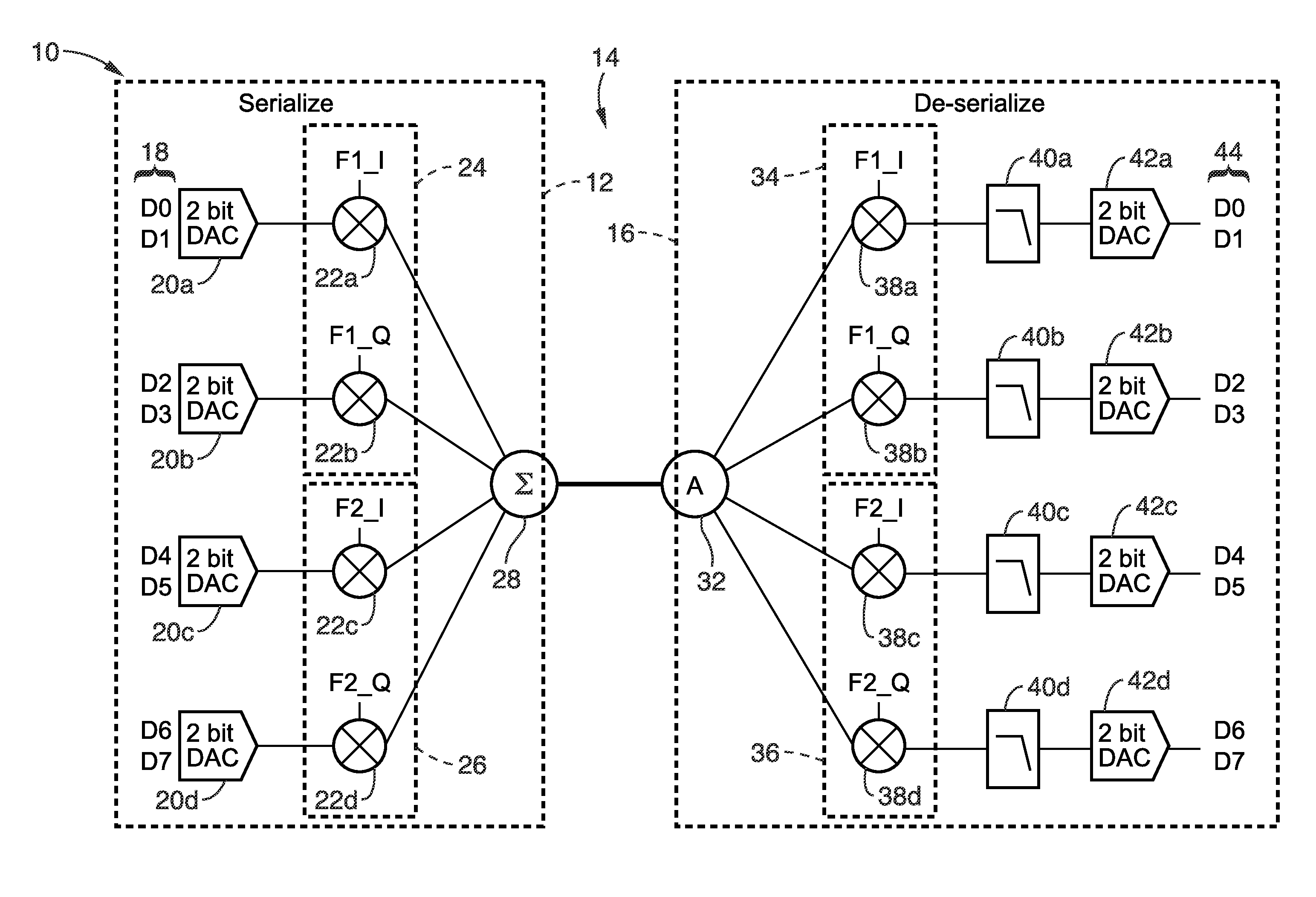
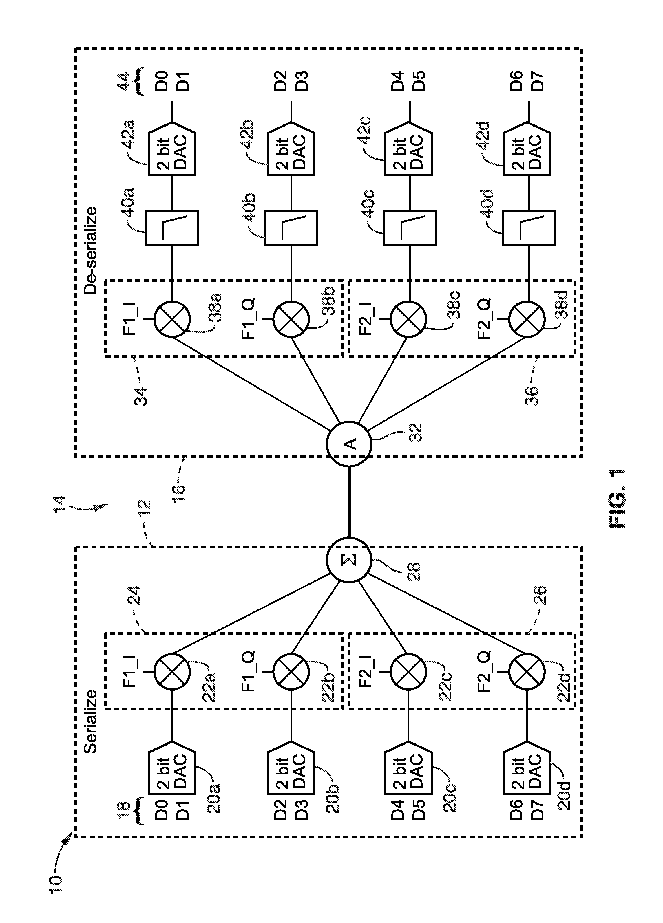
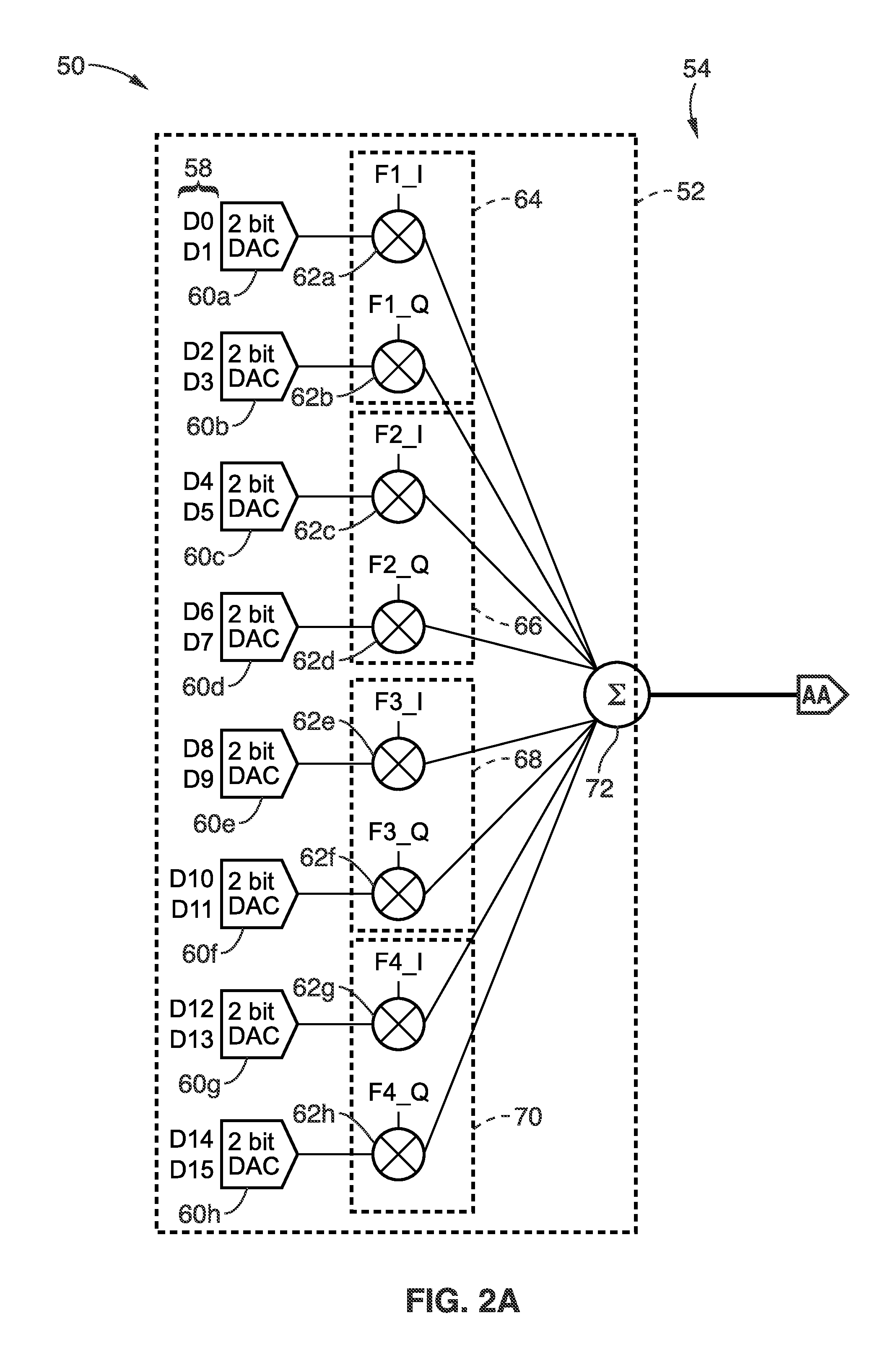
[0017]FIG. 1 illustrates an example embodiment 10 of chip-to-chip communications between a first chip 12 over an I / O connect 14 to a second chip 16. The chip-to-chip communication is performed by serializing parallel digital data (having N bits) onto an analog signal (sum of M analog signals) which is communicated to a second chip, where the analog signal is de-serialized back into parallel digital data. The communication in this embodiment utilizes multiple (e.g., two) frequency bands encoded with a quadrature amplitude modulation (e.g., QAM) scheme to serialize and de-serialize data through an input-output chip connection, providing chip-to-chip communications. Embodiments of the present invention can utilize more than two frequency bands into which the digital data is encoded. It should be appreciated that one of these modulation frequencies can be zero, that is DC. Using DC as one modulation frequency can reduce the number of frequency generation circuits needed, including phase...


PUM


Abstract

A serializer and de-serializer circuit which is particularly well-suited for use in communicating digital data from one integrated circuit (chip) to another for implementing chip-to-chip communications is presented. The circuits are scalable and utilize a multi-frequency quadrature amplitude modulation (QAM) mechanism for converting digital data bits from a parallel form into a serial analog stream for communication over a chip I / O connection. The serializer has multiple digital-to-analog converters (DACs) whose outputs are directed to QAM mixer inputs, within QAMs at multiple frequencies, whose outputs are summed into a single analog signal for communication over an I / O connection. The de-serializer amplifies the analog signal which is received by QAM mixers at different frequencies, whose outputs are low pass filtered and converted back to parallel digital data bits.

Description

CROSS-REFERENCE TO RELATED APPLICATIONS[0001]This application is a 35 U.S.C. §111(a) continuation of PCT international application number PCT / US2013 / 066190 filed on Oct. 22, 2013, incorporated herein by reference in its entirety, which claims priority to, and the benefit of, U.S. provisional patent application Ser. No. 61 / 723,282 filed on Nov. 6, 2012, incorporated herein by reference in its entirety. Priority is claimed to each of the foregoing applications.[0002]The above-referenced PCT international application was published as PCT International Publication No. WO 2014 / 074300 on May 15, 2014, which publication is incorporated herein by reference in its entirety.STATEMENT REGARDING FEDERALLY SPONSORED RESEARCH OR DEVELOPMENT[0003]This invention was made with Government support under 0926127, awarded by the National Science Foundation. The Government has certain rights in the invention.INCORPORATION-BY-REFERENCE OF MATERIAL SUBMITTED IN A COMPUTER PROGRAM APPENDIX[0004]Not Applicab...

Claims


Application Information

Patent Timeline
Patent Type & Authority Patents(United States)
IPC IPC(8): H04L25/00H04L27/36H03M9/00H04L27/00H04L27/38
CPCH03M9/00H04L27/0002H04L27/362H04L27/38
Inventor LEE, SHEAU JIUNGCHANG, MAU-CHUNG FRANKKIM, YANGHYO
Owner RGT UNIV OF CALIFORNIA
Why Eureka
Try Eureka