Substrate manufacturing method

a manufacturing method and substrate technology, applied in the direction of cable/conductor manufacturing, printed circuit manufacturing, conductive pattern formation, etc., can solve the problems of resin not always having a sufficient characteristic, connection failure, and need for expensive laser machining equipment, etc., to simplify the manufacturing process, optimize wettability, and cost relatively low

Inactive Publication Date: 2016-06-28
MEIKO ELECTRONICS CO LTD
View PDF8 Cites 0 Cited by
  • Summary
  • Abstract
  • Description
  • Claims
  • Application Information

AI Technical Summary

Benefits of technology

[0012]According to the present invention, since the insulating layer is formed by the inkjet system, it is possible to form the via hole simultaneously with the formation of the insulating layer. Consequently, a step of separately forming a via hole with a laser or the like is unnecessary, expenses are relatively low, and it is possible to simplify a manufacturing process.
[0013]The first insulating resin is ultraviolet curing resin, and, immediately after the first insulating resin impacts on the surface of the insulating base material, an ultraviolet ray is irradiated on the impact position. Therefore, it is possible to prevent the first insulating resin from wetting and spreading more than necessary.
[0014]After the first insulating resin is impacted on a position surrounding a position to be formed as the via hole, the first insulating resin is cured to form a bank section, and, thereafter, the insulating layer is formed. Therefore, the position of the via hole is set in advance by the bank section. Consequently, it is possible to surely form the via hole.
[0015]Corona treatment, low-pressure UV irradiation treatment, or plasma treatment is applied to the surface of the insulating base material on which the inner layer circuit is formed. Therefore, it is possible to perform surface reforming of the insulating base material and optimize wettability for the first insulating resin. In particular, it is useful to apply such optimization of wettability to an insulating base material in which resin and copper are mixed. The corona treatment is preferable when costs of an apparatus, running costs, and the like are taken into account.
[0016]A resist layer is formed by the inkjet system. Therefore, it is possible to form a resist layer in which a via hole portion is opened. A step for separately opening a via hole portion in a resist is unnecessary.

Problems solved by technology

However, in these methods, when the laser is used, an expensive laser machining apparatus is necessary.
Some laser machining conditions may cause a connection failure.
When photosensitive resin is used, the resin does not always have a sufficient characteristic as a material to be formed as an insulating layer of a substrate and does not have a degree of freedom of material selection.
Photosensitive resin that can be used for the substrate is generally expensive.

Method used


Image

  • Substrate manufacturing method
  • Substrate manufacturing method
  • Substrate manufacturing method

Examples


Embodiment Construction

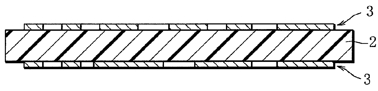
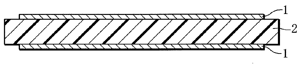
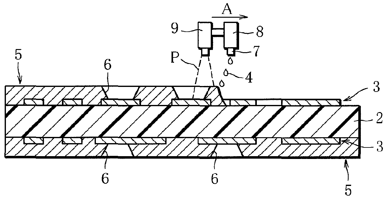
[0027]In a substrate manufacturing method according to the present invention, first, an inner layer circuit forming step is performed. In the inner layer circuit forming step, first, as shown in FIG. 1, an insulating base material 2, on both surfaces of which metal films 1 are stuck, is prepared. For example, the metal films 1 are copper foils. As shown in FIG. 2, the metal films 1 are partially removed to form a patterned inner layer circuit 3.

[0028]Subsequently, an insulating layer forming step is performed. In the insulating layer forming step, as shown in FIG. 3, first insulating resin 4 is applied to each of both the surfaces of the insulating base material 2 by an inkjet system to form an insulating layer 5. The first insulating resin 4 is sprayed from a nozzle 7 of a spraying device 8 using a publicly known inkjet apparatus and impacts on the insulating base material 2 (or the inner layer circuit 3). The nozzle 7 moves in one direction with respect to the insulating base mate...


PUM

PropertyMeasurementUnit
thicknessaaaaaaaaaa
viscosityaaaaaaaaaa
pressureaaaaaaaaaa

Abstract

A substrate manufacturing method includes an inner layer circuit forming step for partially removing metal films from an insulating base material (2), on both surfaces of which the metal films are stuck, and forming an inner layer circuit (3); and an insulating layer forming step for applying first insulating resin (4) to each of both the surfaces of the insulating base material (2) with an inkjet system and forming an insulating layer (5). In the insulating layer forming step, a via hole (6) from which the inner layer circuit (3) is partially exposed is formed simultaneously with the application of the first insulating resin (4). Consequently, a step of separately forming a via hole with a laser or the like is unnecessary, expenses are relatively low, and it is possible to simplify a manufacturing process.

Description

TECHNICAL FIELD[0001]The present invention relates to a substrate manufacturing method using an inkjet technique.BACKGROUND ART[0002]Conventionally, when a multilayer substrate (HDI) is manufactured in which high-density connection is realized by formation of via holes, in formation of an insulating layer of the multilayer substrate, a prepreg and a copper foil are laminated and cured by vacuum press or the like, the copper foil in a via hole forming portion is removed by etching or the like, and, then, the via holes are formed by laser machining. Alternatively, surface treatment is applied to the copper foil and the via holes are directly formed by the laser machining.[0003]As another method of forming via holes, there is a method of uniformly applying varnish-like ink resin over the entire both surfaces of a rigid core substrate with screen printing, a curtain coat, a roll coater, a spray, or the like and, then, forming the via holes with exposure and development (when the resin i...

Claims


Application Information

Patent Timeline
Patent Type & Authority Patents(United States)
IPC IPC(8): H01B13/00C23F1/00H05K3/12H01L21/768C03C25/00B23P15/00H05K3/46H05K3/34
CPCH05K3/125H01L21/76802H05K3/1258H05K3/4673H01L2221/101H05K3/3452H05K2203/013H05K2203/10H05K2203/107
Inventor TAKII, SHUKICHITANEKO, NORIAKIMICHIWAKI, SHIGERUKUROSU, MITSUHONAYA, YUICHIRO
Owner MEIKO ELECTRONICS CO LTD
Why Eureka
Try Eureka