Display device

a technology of a display device and a display panel, which is applied in the direction of dielectric characteristics, instruments, optics, etc., can solve the problems of large deformation of the substrate, uneven luminance, warping of the display panel, etc., and achieve the effect of improving the reliability of connection

Active Publication Date: 2016-08-09
JAPAN DISPLAY INC
View PDF11 Cites 0 Cited by
  • Summary
  • Abstract
  • Description
  • Claims
  • Application Information

AI Technical Summary

Benefits of technology

[0009]The invention has been achieved in view of the above described situations, and an object of the invention is to provide a display device with further improved reliability in connection of an ultraviolet curing anisotropic conductive film.

Problems solved by technology

However, with the thermosetting anisotropic conductive film, the display panel can be warped due to heat at pressure-joining and luminance unevenness is caused in display of the display device.
Further, when a touch panel is attached onto the display panel, stress distributions are biased in both the touch panel and the display panel due to warp of the display panel, and further luminance unevenness etc. are caused.
On the other hand, in a sheet display having a substrate of the display device formed using a flexible or bendable material, the substrate largely deforms due to heat and it is difficult to directly use the thermosetting anisotropic conductive film.
However, the terminal on the substrate is formed using a light-blocking metal, and there may be locations in the anisotropic conductive film without sufficient application of ultraviolet light and reliability of connection may be insufficient.

Method used


Image

  • Display device
  • Display device
  • Display device

Examples


Embodiment Construction

[0026]As below, respective embodiments of the invention will be explained with reference to the drawings. Note that the disclosure is just an example and the scope of the invention naturally includes appropriate changes that could be readily achieved while keeping the spirit of the invention. Further, in the drawings, for clearer explanation, widths, thicknesses, shapes, etc. of respective parts may be schematically shown compared to the actual forms, however, they are just examples and do not limit the interpretation of the invention. Furthermore, in the specification and the drawings, the same signs are assigned to the similar elements previously described with respect to the previously mentioned drawings, and the detailed explanation may be appropriately omitted.

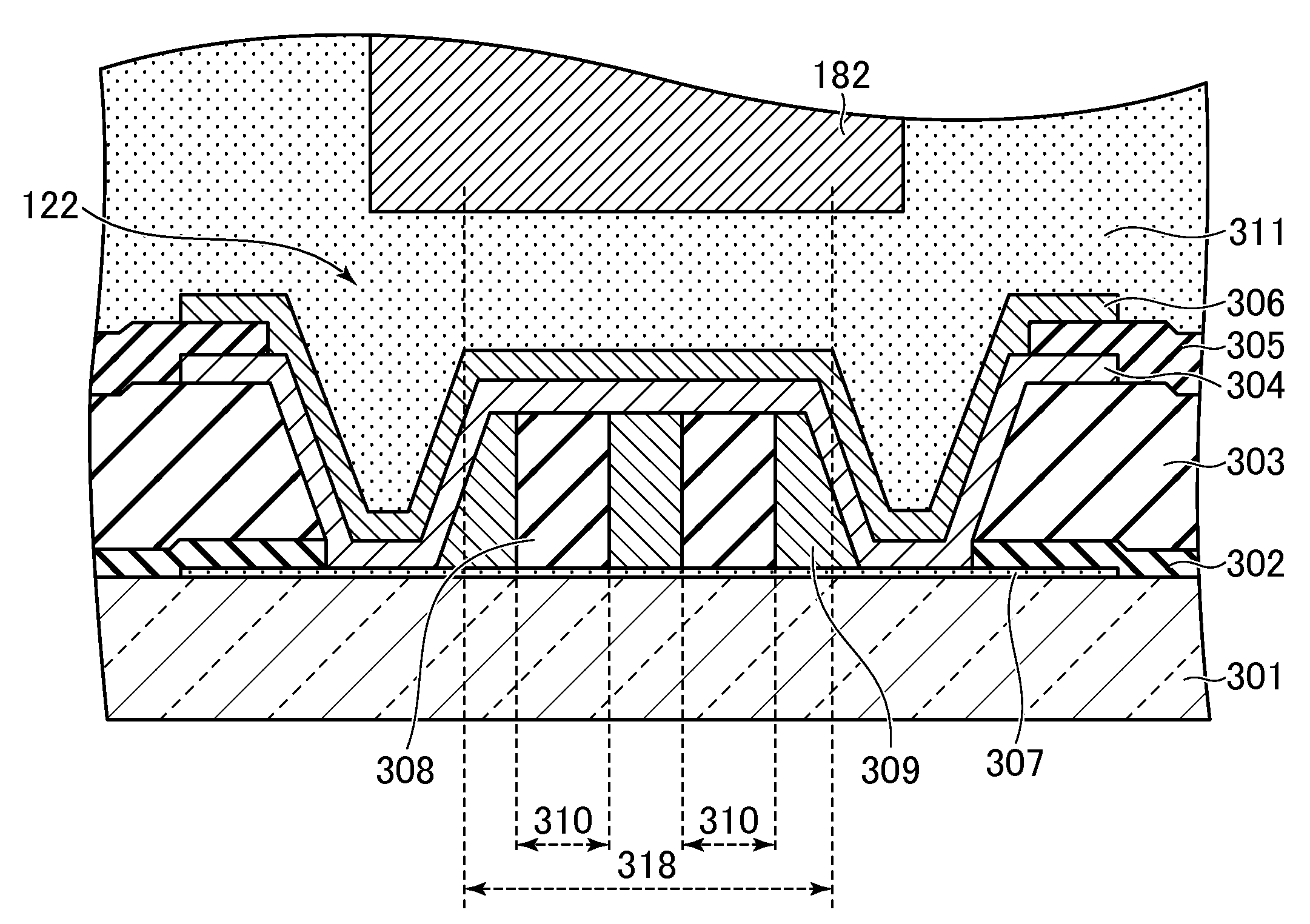
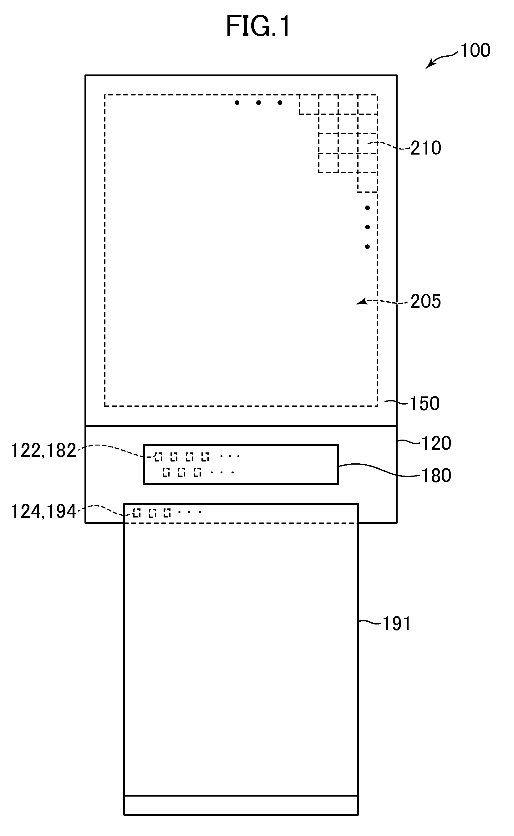
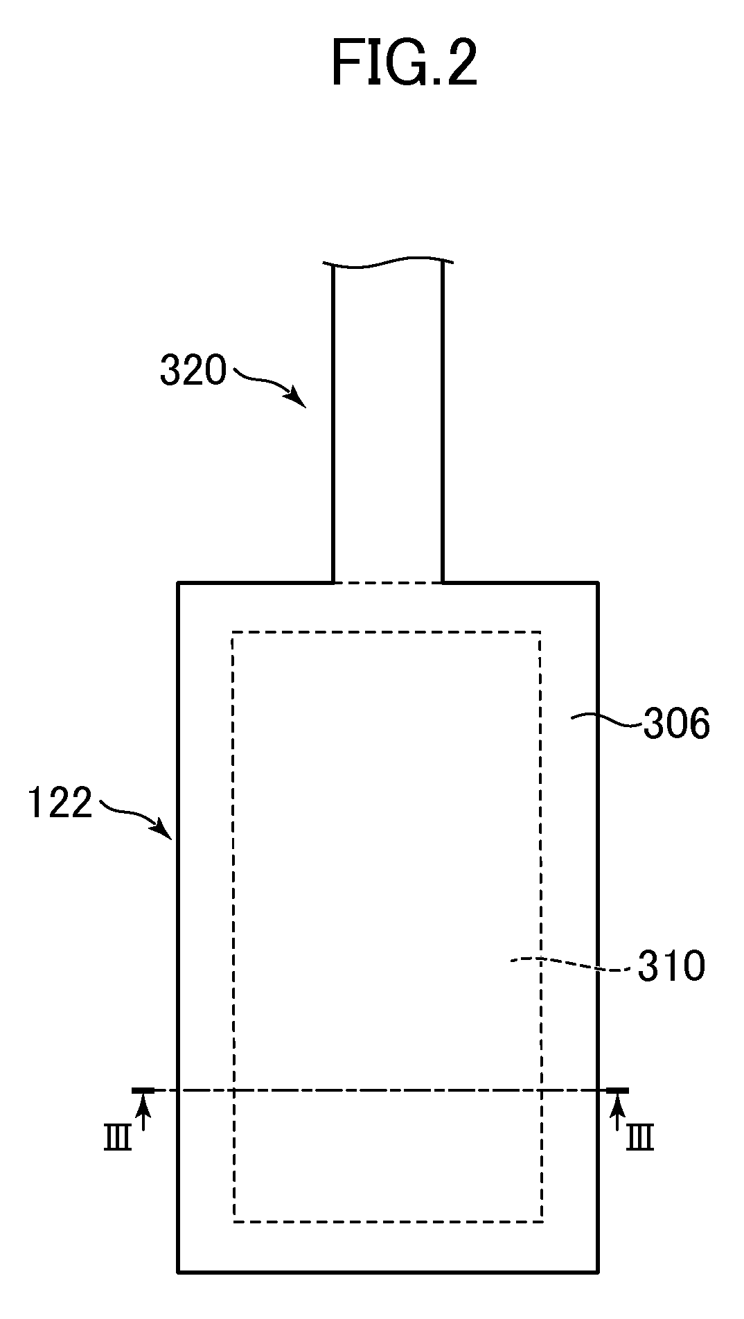
[0027]FIG. 1 schematically shows a display device 100 according to an embodiment of the invention. As shown in the drawing, the display device 100 has two substrates of a TFT (Thin Film Transistor) substrate 120 and an op...


PUM

PropertyMeasurementUnit
transparentaaaaaaaaaa
anisotropic conductiveaaaaaaaaaa
conductiveaaaaaaaaaa

Abstract

A display device includes a substrate on which a plurality of pixels are arranged and a circuit for displaying images with respect to each pixel is formed, a substrate terminal as a terminal formed on the substrate, and an electronic component terminal as a terminal of an electronic component electrically connected to the terminal via an anisotropic conductive film. A conductive region that conducts to the anisotropic conductive film in the substrate terminal has a light transmissive part in which a material having light transmissivity penetrates the substrate surface in a perpendicular direction.

Description

CROSS-REFERENCE TO RELATED APPLICATION[0001]The present application claims priority from Japanese application JP2014-078981 filed on Apr. 7, 2014, the content of which is hereby incorporated by reference into this application.BACKGROUND OF THE INVENTION[0002]1. Field of the Invention[0003]This invention relates to a display device.[0004]2. Description of the Related Art[0005]As display devices such as information communication terminals including computers and television receivers, liquid crystal display devices are widely used. Further, organic EL (Electro-Luminescent) display devices are also known as thin display devices. The display panel of the thin display device performs display by operating TFTs (Thin Film Transistors) formed on respective pixels of a display area on a substrate. Here, the TFT is driven by a drive IC (Integrated Circuit) as a semiconductor integrated circuit element mounted outside of the display area, and generally, the terminal of the drive IC (bump) and w...

Claims


Application Information

Patent Timeline
Patent Type & Authority Patents(United States)
IPC IPC(8): H01L27/32H01L27/12G02F1/1345H01L25/18H05K1/11H05K3/32H05K1/03
CPCH01L25/18H01L27/124H01L27/1248G02F1/1345H05K1/0306H05K1/111H05K3/323H05K2201/0326H05K2201/10128H05K2201/0104H01L27/3253H01L27/3248H01L2924/0002H01L2924/00H10K59/123H10K59/1275
Inventor ASAKA, TSUNEYUKI
Owner JAPAN DISPLAY INC
Why Eureka
Try Eureka