
Method and apparatus for microwave treatment of dielectric films

a dielectric film and microwave treatment technology, applied in the direction of microwave heating, electric apparatus, basic electric elements, etc., can solve the problems of poor adhesion with adjacent layers, reduced cohesive strength of porous dielectrics, and numerous challenges of porous dielectrics, so as to enhance the reaction in the film material, reduce the thermal budget, and enhance the coupling with microwaves

Active Publication Date: 2016-08-09
APPLIED MATERIALS INC
View PDF19 Cites 29 Cited by
  • Summary
  • Abstract
  • Description
  • Claims
  • Application Information

AI Technical Summary

Benefits of technology

This approach effectively reduces thermal processing requirements, enhances mechanical and electrical properties, and prevents physical and surface damage during semiconductor fabrication, improving the robustness and performance of low-k dielectric films.

Problems solved by technology

However, successful implementation of these porous dielectrics structures poses numerous challenges.
As compared to their dense counterparts, porous dielectrics are expected to have reduced cohesive strength and poorer adhesion with adjacent layers.
The ingress of water into the dielectric negatively impacts both the mechanical integrity as well as electrical performance of the devices.
Another challenge for these porous OSG low-k dielectrics is that they are susceptible to damage induced during etching and cleaning process, which degrades the dielectric and electrical properties and surface roughness.
However, after the plasma processes have been performed this temporary material has to be removed or burnt out to recreate the pores and have a low k dielectric film.

Method used


Image

  • Method and apparatus for microwave treatment of dielectric films
  • Method and apparatus for microwave treatment of dielectric films
  • Method and apparatus for microwave treatment of dielectric films

Examples


example

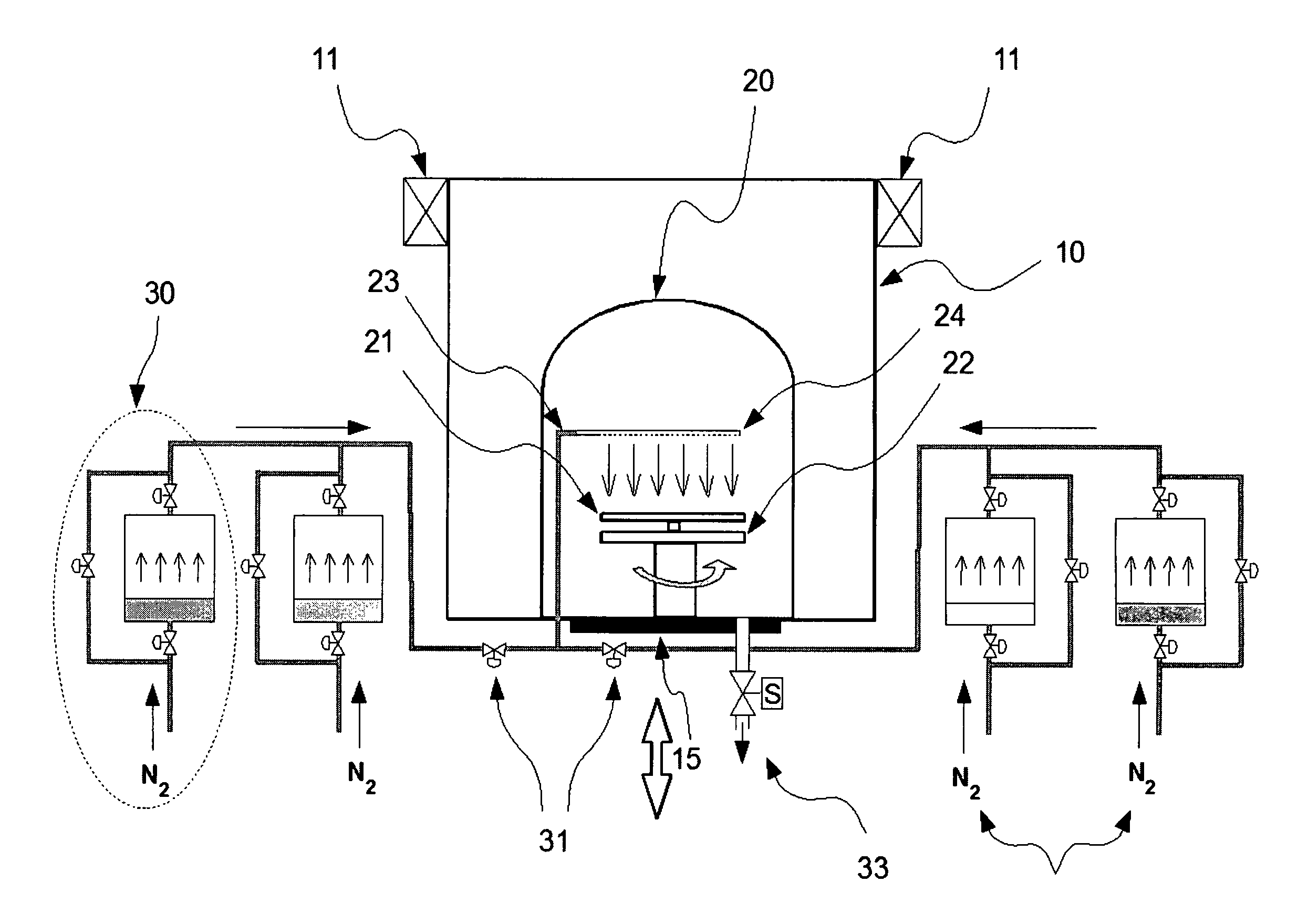
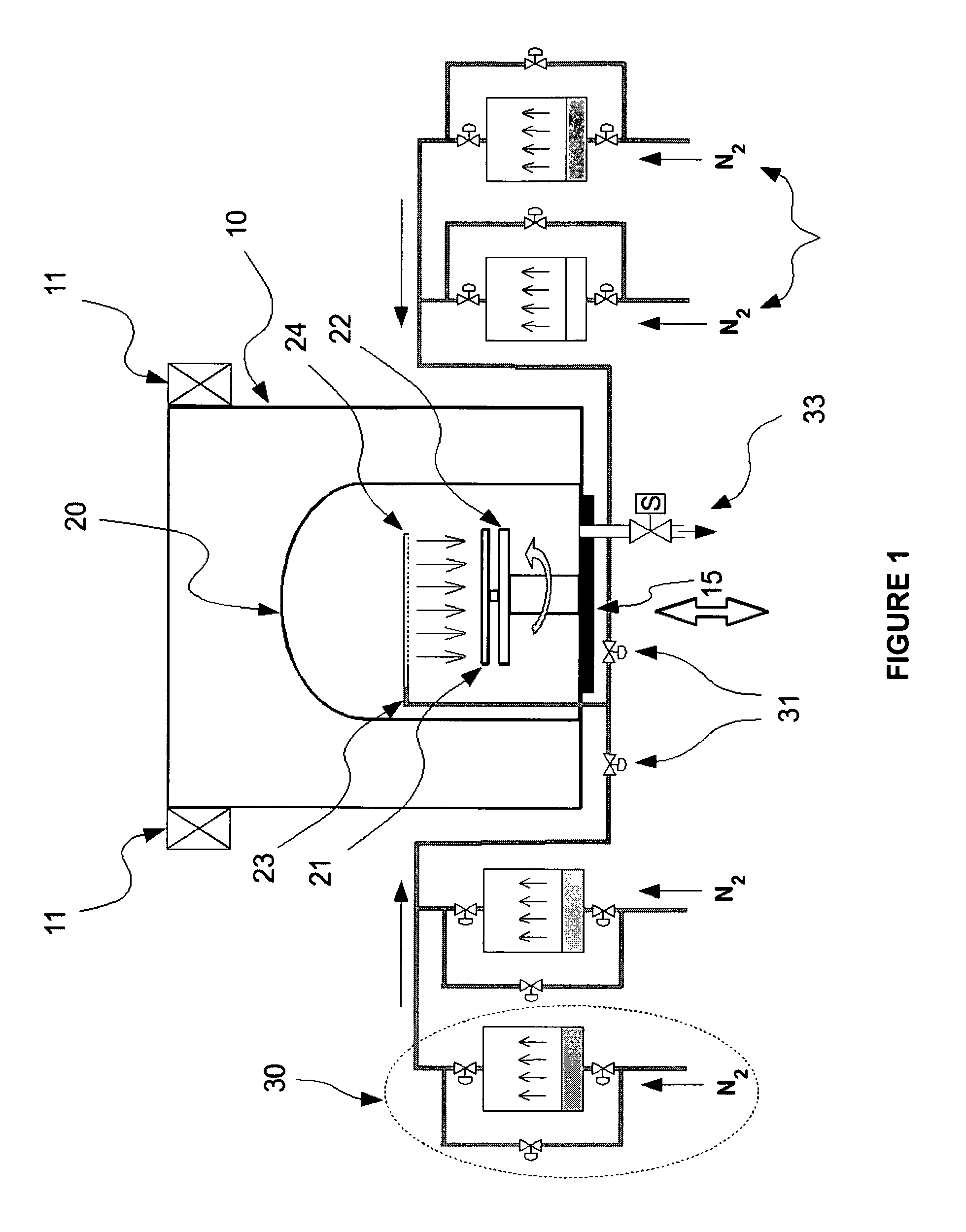
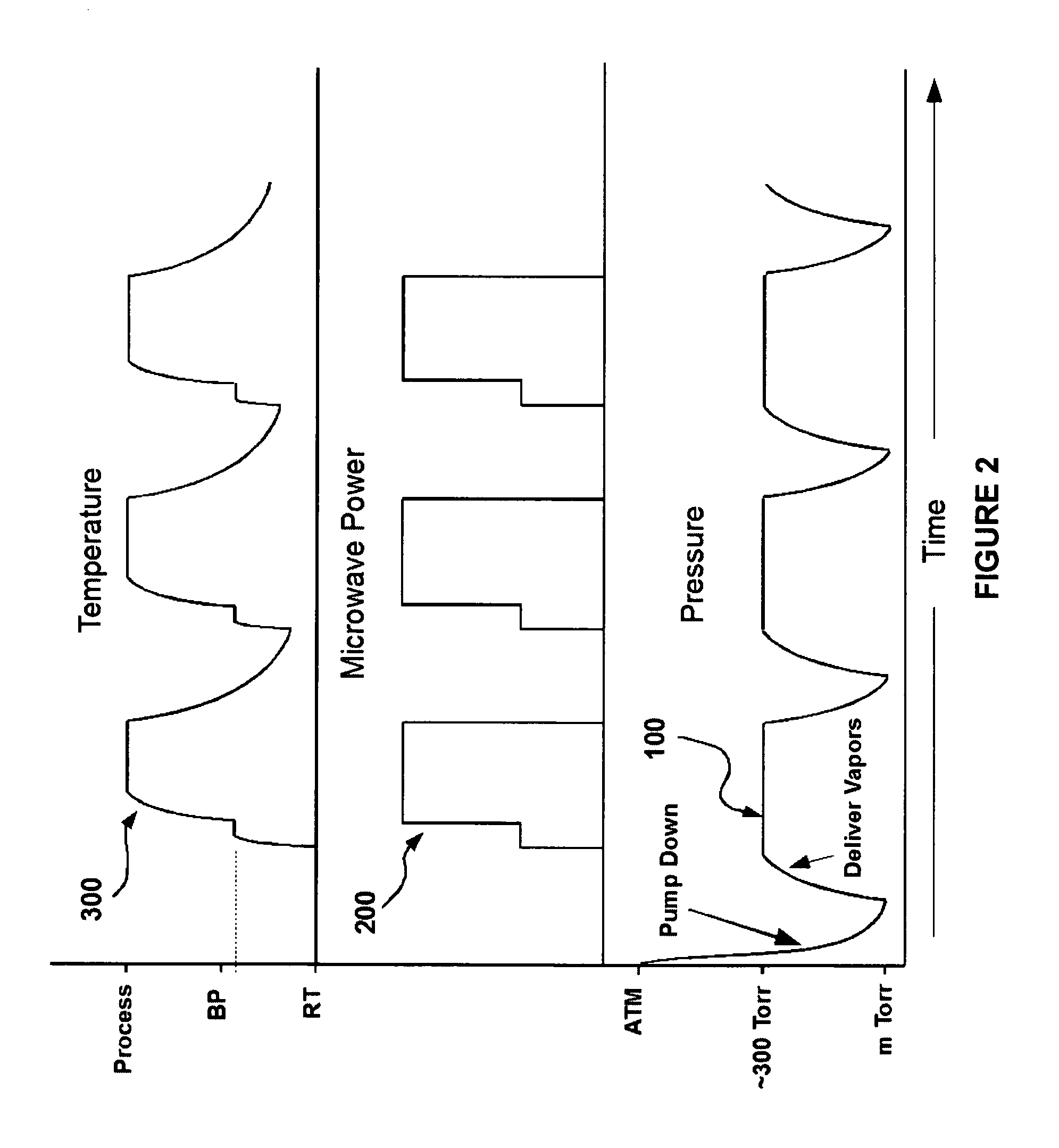
[0082]A porous dielectric film containing PMMA stuffed into the pores was placed in a vacuum capable microwave chamber and first pumped down to 5×10⁻⁵ Torr at which point 500 sccm flow of N2 was allowed, which brought the pressure up to 6×10⁻² Torr. Then microwave power was delivered into the chamber and the temperature was increased to soak temperatures of 330, 370 and 410° C. The purpose of this brief higher temperature step was to partially create the pores by partial burnout of PMMA.

[0083]The time (m=minutes) at temperature is half of what is shown in the data on FIGS. 4 and 5. The N and EW in FIGS. 4 and 5 stand for “No” conditioning and using “ethanol+water” mixture (E:W=60:40 by weight) as the solvent. The largest peak in FIG. 5 is for the dielectric film sample with PMMA still stuffed in it, while ALKB refers to the Pristine OSG film.

[0084]After the first exposure to microwave and half the soak time at high temperature, the sample was cooled to room temperature and immersed ...


PUM

PropertyMeasurementUnit
temperatureaaaaaaaaaa
porosityaaaaaaaaaa

Abstract

A method for processing a dielectric film on a substrate comprises: depositing a porous dielectric film on a substrate; removing the porogen; stuffing the film with a protective polymeric material; performing at least one intermediate processing step on the stuffed dielectric film; placing the film in a microwave applicator cavity and heating to a first temperature to partially burn out the polymeric material; introducing a controlled amount of a polar solvent into the porosity created by the partial burn out; applying microwave energy to heat the film to a second selected temperature below the boiling point of the solvent to clean away remaining polymeric material; and applying microwave energy to heat the film to a third temperature above the boiling point of the solvent to completely burnout the residues of polymeric material. The interaction of the polar solvent with the microwaves enhances the efficiency of the cleaning process.

Description

CROSS REFERENCE TO RELATED APPLICATIONS[0001]This application claims the benefit of Provisional Application Ser. No. 61 / 854,556, filed Apr. 26, 2013 by the present inventor, the entire disclosure of which is incorporated herein by reference. The application is further related to the following utility applications, all filed on even date herewith: Method and Apparatus for Microwave Treatment of Dielectric Films, U.S. patent application Ser. No. 14 / 120,011, and Method and Apparatus for Microwave Treatment of Dielectric Films, U.S. patent application Ser. No. 14 / 120,010, the entire disclosures of which are incorporated herein by reference.BACKGROUND OF THE INVENTION[0002]1. Field of the Invention[0003]The invention pertains to apparatus and method for tailored microwave heat treatment of low dielectric constant (k) organo-silicate glass (OSG) films deposited on substrates for semiconductor devices. More particularly, the invention pertains to burnout of post porosity plasma protection ...

Claims


Application Information

Patent Timeline
Patent Type & Authority Patents(United States)
IPC IPC(8): H01L21/00H01L21/02H01L21/268H01L21/67H05B6/80
CPCH05B6/80H01L21/02203H01L21/02321H01L21/2686H01L21/02345H01L21/02359H01L21/67115H01L21/67167
Inventor AHMAD, IFTIKHARBAKLANOV, MIKHAILZHANG, LIPING
Owner APPLIED MATERIALS INC
Learn More