
Photosensitive element, method for forming resist pattern, and method for producing printed circuit board

a technology of resist pattern and photosensitive element, which is applied in the direction of photosensitive materials, circuit masks, instruments, etc., can solve the problems of difficult removal of bonded phototools, inability to meet the high resolution requirements of photosensitive films, etc., and achieves satisfactory adhesiveness and resolution, sufficiently reduced microdefects of resists, and rectangular cross-sectional shape

Active Publication Date: 2016-09-06
RESONAC CORPORATION
View PDF48 Cites 1 Cited by
  • Summary
  • Abstract
  • Description
  • Claims
  • Application Information

AI Technical Summary

Benefits of technology

The solution enables the formation of resist patterns with enhanced adhesiveness, resolution, and reduced microdefects, suitable for substrates with surface roughness below 300 nm, leading to higher production yields and more rectangular resist shapes, even for high-density printed wiring boards.

Problems solved by technology

Conventional support films therefore have increased haze, and the fine particles in the support film tend to cause light scattering under light exposure, so that the requirement for high resolution of the photosensitive film cannot be met.
However, since the photosensitive layer usually has some level of pressure-sensitive adhesive property, it is difficult to remove the bonded phototool when exposure is carried out after directly bonding a phototool onto the photosensitive layer.

Method used


Image

  • Photosensitive element, method for forming resist pattern, and method for producing printed circuit board
  • Photosensitive element, method for forming resist pattern, and method for producing printed circuit board
  • Photosensitive element, method for forming resist pattern, and method for producing printed circuit board

Examples


synthesis example 1

[0175]In a flask equipped with a stirrer, reflux condenser, thermometer, dropping funnel and nitrogen gas inlet tube there was added 420 g of a mixture of toluene and methylcellosolve in a weight ratio of 6:4, and the mixture was stirred while blowing in nitrogen gas and heated to 80° C. Separately, as copolymerizing monomer there was prepared a mixed solution of 162 g of methacrylic acid, 30 g of methyl methacrylate, 270 g of styrene, 270 g of benzyl methacrylate and 4.4 g of azobisisobutyronitrile (hereinafter referred to as “solution a”), and, over a period of 4 hours, solution “a” was added dropwise to the mixture of toluene and methylcellosolve in a weight ratio of 6:4, that had been heated to 80° C. Next, 40 g of the mixture of toluene and methylcellosolve in a weight ratio of 6:4 was used for rinsing of the dropping funnel and added into the flask, and heating was then performed for 2 hours while stirring at 80° C. Also, a solution of 1.0 g of azobisisobutyronitrile dissolved...

synthesis example 2

[0176]A binder polymer solution as component (a) was obtained by the same procedure as Synthesis Example 1, except that as the copolymerizing monomer there was prepared a mixed solution of 150 g of methacrylic acid, 300 g of methyl methacrylate, 150 g of styrene and 4.4 g of azobisisobutyronitrile (hereunder referred to as “solution b”). Toluene was added to the binder polymer solution to adjust the non-volatilizing component concentration (solid concentration) to 40 wt %. The weight-average molecular weight of the binder polymer was 45000. The acid value of the binder polymer was 121 mgKOH / g.

[0177](GPC Conditions)

Pump: Hitachi L-6000 (trade name of Hitachi, Ltd.).

Column: Gelpack GL-R420+Gelpack GL-R430+Gelpack GL-R440M (total: 3) (all trade names of Hitachi Chemical Co., Ltd.)

Eluent: tetrahydrofuran

Measuring temperature: 40° C.

Flow rate: 2.05 mL / min

Detector: Hitachi L-3300 RI (trade name of Hitachi, Ltd.).

[0178](Measurement of Acid Value)

[0179]Synthesized binder polymer was weighed...


PUM

PropertyMeasurementUnit
Raaaaaaaaaaa
diametersaaaaaaaaaa
wt %aaaaaaaaaa

Abstract

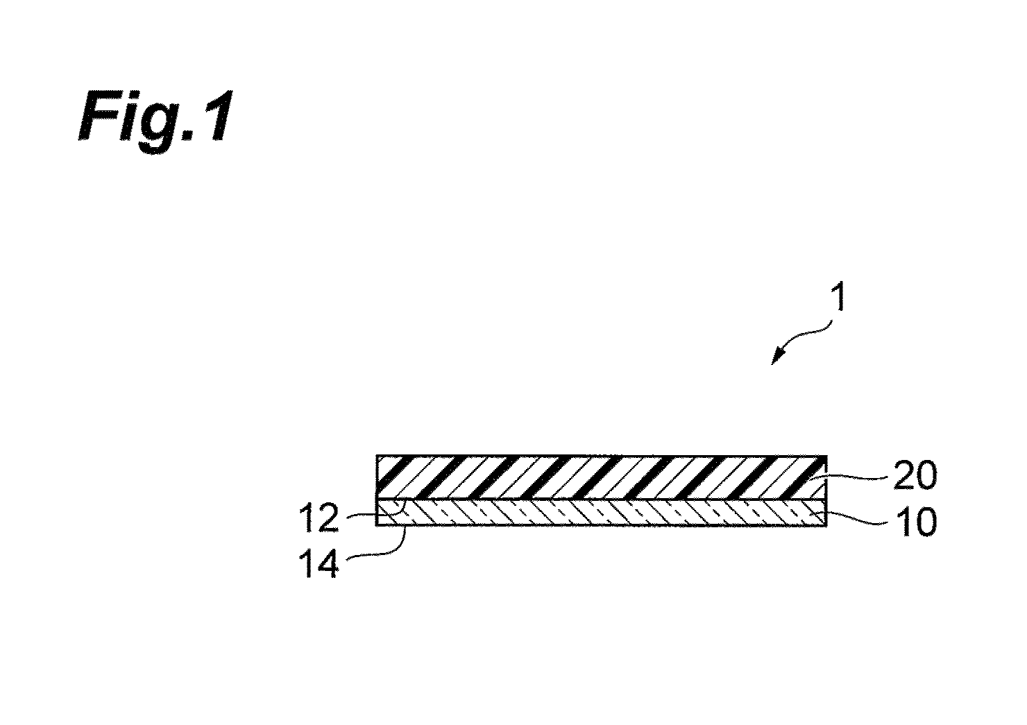
The invention relates to a photosensitive element comprising a support film and a photosensitive layer derived from a photosensitive resin composition formed on the support film, wherein the support film haze is 0.01-1.5%, the total number of particles with diameters of 5 μm and larger and aggregates with diameters of 5 μm or larger in the support film is no greater than 5 / mm2, the photosensitive layer contains a binder polymer, a photopolymerizable compound with an ethylenically unsaturated bond and a photopolymerization initiator, and the thickness T of the photosensitive layer and the absorbance A of the photosensitive layer at 365 nm satisfies the relationship represented by inequality (I):0.001≦A / T≦0.020  (I).

Description

[0001]This is a National Phase Application in the United States of International Patent Application No. PCT / JP2011 / 079097 filed Dec. 15, 2011, which claims priority on Japanese Patent Application No. P2010-280604, filed Dec. 16, 2010.FIELD OF THE INVENTION[0002]The present invention relates to a photosensitive element, and to a method for forming a resist pattern and a method for producing a printed wiring board, which employ it.BACKGROUND OF THE INVENTION[0003]The fields of manufacturing conventional printed wiring boards and precision working of metals widely employ photosensitive elements comprising a layer made of a photosensitive resin composition (“photosensitive layer”), a support film and a protective film, as resist materials for etching, plating and the like.[0004]A printed wiring board may be manufactured, for example, in the following manner. First, the protective film of a photosensitive element is released from the photosensitive layer and the photosensitive layer is t...

Claims


Application Information

Patent Timeline
Patent Type & Authority Patents(United States)
IPC IPC(8): G03F7/09G03F7/085G03F7/033G03F7/031H05K3/00H05K3/06G03F7/20G03F7/40G03F7/16
CPCH05K3/064G03F7/031G03F7/033G03F7/085G03F7/09G03F7/20G03F7/40H05K3/0076
Inventor KUBOTA, MASAO
Owner RESONAC CORPORATION
Learn More