Multi-spot illumination for improved detection sensitivity

a multi-spot illumination and detection sensitivity technology, applied in the direction of optical radiation measurement, lighting and heating apparatus, instruments, etc., can solve the problems of excessive heat generation by the interaction of incident optical radiation with the wafer surface, the power density of the incident laser beam is capable of damaging the wafer surface, and the substrate damage is primarily related, so as to achieve a uniform illumination profile and minimize interference

Active Publication Date: 2016-11-15
KLA CORP
View PDF41 Cites 0 Cited by
  • Summary
  • Abstract
  • Description
  • Claims
  • Application Information

AI Technical Summary

Benefits of technology

[0016]Methods and systems for minimizing interference among multiple illumination beams generated from a non-uniform illumination source to provide an effectively uniform illumination profile over the field of view of an inspection system are presented.
[0017]In one aspect, interferences among the multiple illumination beams are effectively mitigated by employing an optical subsystem that generates multiple illumination beams from a pulsed illumination source having a non-uniform intensity distribution. The optical subsystem introduces optical delay among the multiple illumination beams at the surface of the specimen under inspection. Since the multiple beams illuminating the surface are temporally separated, interference among the illumination beams at the detector is minimized.
[0018]In another aspect, interferences among the multiple illumination beams are effectively mitigated by employing a time-delay integration (TDI) detector and an optical subsystem that generates multiple illumination beams from an illumination source having a non-uniform intensity distribution. The optical subsystem directs each of the multiple illumination beams to the surface of the specimen under inspection such that each area of the surface of the specimen illuminated by each beam is spatially separate from the others. The TDI detector receives an amount of light collected from each area of the specimen illuminated by each of the illumination beams. A point object imaged by the optical system onto the TDI detector moves across the detector surface with the same speed as the speed of transfer of charges through the detector. Since each illumination area is spatially separated, the point object of interest moves through any illumination areas in the path of the motion trajectory of the point object without interference. The image of the point object illuminated by each illumination area in its path moves across the TDI detector as the associated charge coupled device (CCD) charges are transferred across the detector. Thus, the point object of interest will interact with illumination light from each illumination spot in its motion trajectory and the interaction will be passed to the TDI detector, and integrated. In this manner, the relative position of the illumination spots along the direction of motion of the point object of interest has no impact on the illumination efficiency distribution over the field of view.
[0021]In some embodiments, an optical subsystem is employed to spatially split a non-uniform illumination beam into at least two half-beams. In some examples, a pulsed illumination beam is spatially split into at least two half-beams and any spatially overlapping half-beams are delayed in time longer than the pulse length to avoid interference. In these examples, the half-beams are spatially displaced slightly so that the total intensity profile has a flat top around the center. In some examples, this results in a more effective use of illumination light. In addition, the peak intensity of each pulse is reduced and the lifetime of optics and sensors is improved.
[0022]In some embodiments, an illumination beam is incident on a parallel beam plate at a nonzero incident angle and is split into two halves from the center. One part of the beam is directly reflected from the front surface of the plate and the other part of the beam passes through the front surface and is reflected from the back surface. A portion of the reflected beam from the back surface passes through the front surface and another portion is again reflected from the front surface. The added path length creates a spatial shift and also a time delay between any two overlapping beams. Because of the time delay, there is no interference between the beams and the intensity profile integrated within an appropriate period is approximately equal to the sum of the individual intensity profiles.

Problems solved by technology

For example, in high-power, laser-based inspection systems, the power density of the incident laser beam is capable of damaging the wafer surface.
For inspection systems employing a short-pulsed laser illumination source, substrate damage is primarily related to peak power density.
An excessive amount of heat is generated by the interaction of the incident optical radiation with the wafer surface, particularly in areas of incidence subject to incident light with peak power density.
While robust and simple, a significant amount of light is wasted; at significant system cost.
Unfortunately, DOE elements are highly sensitive to periodic phase and intensity fluctuations in the illumination beam profile (wave front errors), and also to position of input beam with respect to DOE.
Furthermore, a manufactured DOE is a fixed optical structure that typically cannot be adapted to accommodate changes in requirements for the final illumination profile.
Similarly, a manufactured DOE cannot be actively altered to respond to changes in phase or intensity distribution of an input beam.
In addition, DOEs are also relatively expensive both to design and manufacture compared to standard optical components, such as spherical lenses and flat mirrors.
However, diffusers share many of the same problems described hereinbefore with respect to DOEs.
In addition, in applications involving coherent illumination, diffusers may give rise to undesired speckle.
However, aspheric optics share many of the same problems described hereinbefore with respect to DOEs.
However, the additional system cost is undesirable.
In general, the disadvantages of existing beam forming systems include low efficiency, sensitivity to aberrations, complexity, and poor flexibility.
However, such manipulations are significantly impacted by interference between the copies, particularly when real-world aberrations of the input beam are taken into account.
The added path length creates a spatial shift and also a time delay between any two overlapping beams.
The path length differences among the half-beams create a spatial shift and also time delay between the beams.

Method used


Image

  • Multi-spot illumination for improved detection sensitivity
  • Multi-spot illumination for improved detection sensitivity
  • Multi-spot illumination for improved detection sensitivity

Examples


Embodiment Construction

[0046]Reference will now be made in detail to background examples and some embodiments of the invention, examples of which are illustrated in the accompanying drawings.

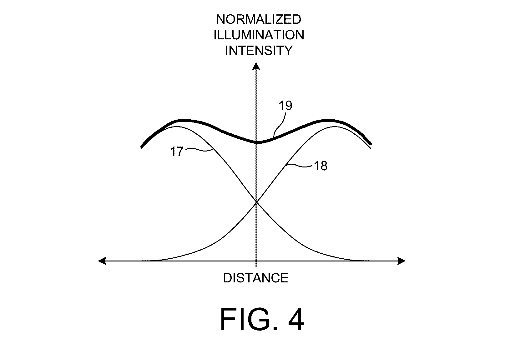
[0047]In one aspect, interferences among the multiple illumination beams are effectively mitigated by employing an optical subsystem that generates multiple illumination beams from a pulsed illumination source having a non-uniform intensity distribution. The optical subsystem introduces an optical delay among the multiple illumination beams at the surface of the specimen under inspection. Since the multiple beams illuminating the surface are temporally separated, interference among the illumination beams at the detector is minimized.

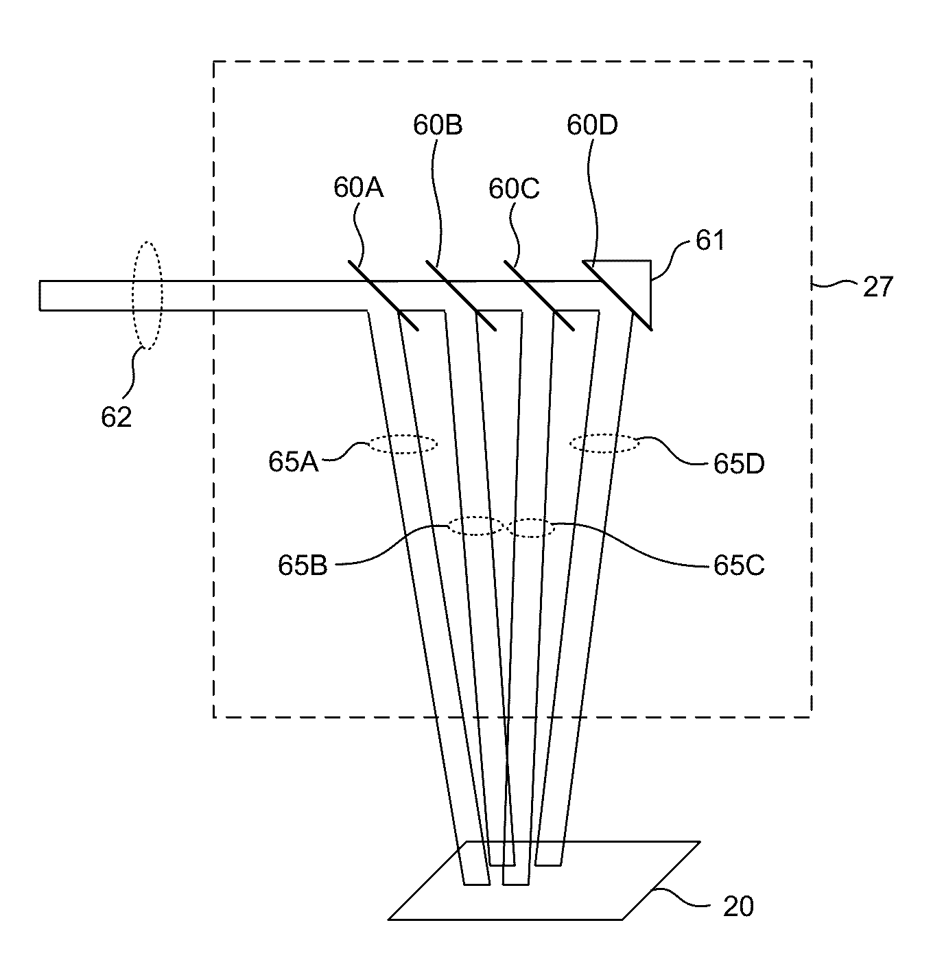
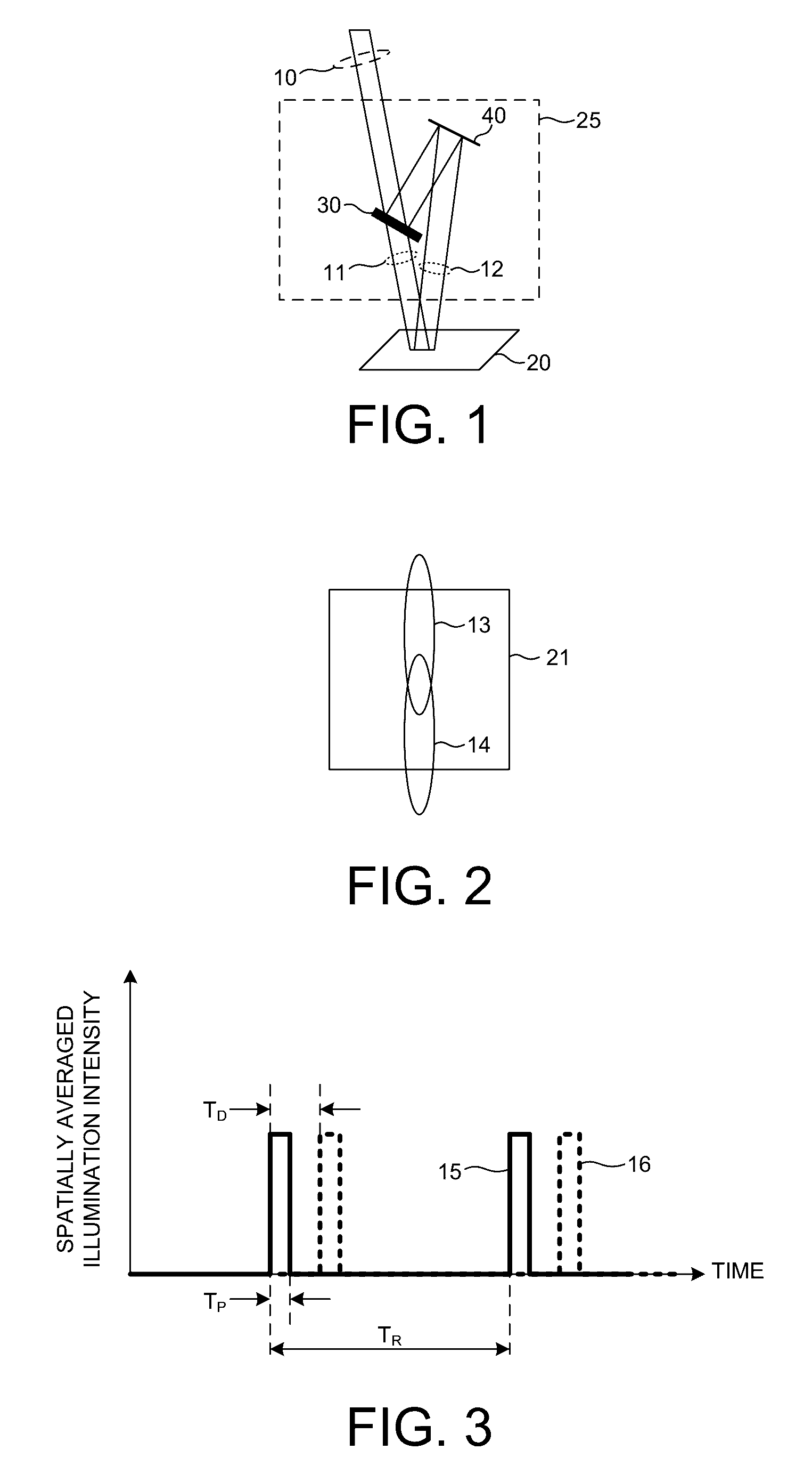
[0048]FIG. 1 depicts an embodiment of an optical subsystem 25 configured to split a beam of incoming illumination light into secondary beams of illumination light that are temporally separated at the surface of the specimen under inspection. Optical subsystem 25 receives an amount of illum...


PUM

PropertyMeasurementUnit
path lengthaaaaaaaaaa
distanceaaaaaaaaaa
angle of incidenceaaaaaaaaaa

Abstract

Methods and systems for minimizing interference among multiple illumination beams generated from a non-uniform illumination source to provide an effectively uniform illumination profile over the field of view of an inspection system are presented. In some examples, a pulsed beam of light is split into multiple illumination beams such that each of the beams are temporally separated at the surface of the specimen under inspection. In some examples, multiple illumination beams generated from a non-uniform illumination source are projected onto spatially separated areas on the surface of the specimen. A point object of interest illuminated by each area is imaged onto the surface of a time-delay integration (TDI) detector. The images are integrated such that the relative position of the illumination areas along the direction of motion of the point object of interest has no impact on the illumination efficiency distribution over the field of view.

Description

CROSS REFERENCE TO RELATED APPLICATION[0001]The present application for patent claims priority under 35 U.S.C. §119 from U.S. provisional patent application Ser. No. 61 / 864,024, entitled “Split Gaussian Beams and Multi-Spot Flat-Top Illumination for Surface Scanning Systems,” filed Aug. 9, 2013, the subject matter of which is incorporated herein by reference.TECHNICAL FIELD[0002]The described embodiments relate to systems for surface inspection, and more particularly to semiconductor wafer inspection modalities.BACKGROUND INFORMATION[0003]Semiconductor devices such as logic and memory devices are typically fabricated by a sequence of processing steps applied to a substrate or wafer. Various features and multiple structural levels of the semiconductor devices are formed by these processing steps. For example, lithography among others is one semiconductor fabrication process that involves generating a pattern on a semiconductor wafer. Additional examples of semiconductor fabrication p...

Claims


Application Information

Patent Timeline
Patent Type & Authority Patents(United States)
IPC IPC(8): G01N21/88G01N21/95G01J1/04
CPCG01N21/9501G01J1/04G01N21/8806F21S2/005F21Y2115/00F21Y2115/30
Inventor CHUANG, YUNG-HO ALEXLU, XIAOXUFIELDEN, JOHNMALEEV, IVAN
Owner KLA CORP
Why Eureka
Try Eureka