LED light module and LED chip

a technology of led light modules and led chips, applied in point-like light sources, lighting and heating apparatuses, light sources, etc., can solve the problems of high manufacturing costs of ain-like high heat conduction ceramics, and high manufacturing costs of led illumination products. , to achieve the effect of reducing internal heat conduction thermal resistance, high voltage insulation, and reducing the cost of led illumination products

Active Publication Date: 2016-11-29
SHENZHEN QIN BO CORE TECH DEV CO LTD
View PDF15 Cites 0 Cited by
  • Summary
  • Abstract
  • Description
  • Claims
  • Application Information

AI Technical Summary

Benefits of technology

[0007]The main object of the present invention is to solve the problem of the internal heat conduction as well as the electrical insulation (especially high voltage insulation) of the LED light module and LED chip, a novel configuration which is based on the principle theory of heat transfer is provided, so as to obtain high voltage insulation and meet higher electro-security regulations while reduce the internal heat conduction thermal resistance in order to significantly reduce the total manufacturing costs without the need for adopting expensive AIN like high heat conduction ceramics.
[0014]The heat dispreading plate which is used for heat dispreading not only needs to adopt a material with a high thermal conductivity, but also the area and thickness thereof should be large enough. The area of the heat dispreading plate should be five times larger than the sum area of the LED wafers on the heat dispreading plate so that the heat-flux density can be reduced five times, preferably ten times in practical applications, the thickness of the heat dispreading plate should be larger than 0.4 mm by means of calculation and analysis by synthesis. The aim and effect of a thick heat dispreading plate is to effectively spread the heat in the heat dispreading plate so as to reduce the heat flux density.
[0016]The ceramic wafer which is sintered into ceramics is compact in substance and has high insulation strength and enough high thermal conductivity, so that the present invention adopts the ceramic wafer which is sintered into ceramics as the high-voltage insulation plate. The alumina ceramic wafer has low manufacturing costs and enough high thermal conductivity, the thermal conductivity of 96 alumina ceramics can be 20 W / m·k, so that it is a first choice of the material for the high-voltage insulation plate.
[0017]The thickness of the ceramic wafer of the high-voltage insulation plate of the present invention is not less than 0.15 mm. From one aspect considering the difficulty of the manufacturing process, the ceramic wafer which is too thin is not easy for producing and is easy to break. From another aspect considering the insulation strength, the insulation strength of the high-voltage insulation plate is defined to be more than 1500V. High insulation strength is beneficial for reducing the power driver circuit, for example, when the insulation strength is high enough to meet the electrical security requirements, a non isolated power driver circuit can be used, the manufacturing costs can be reduced.

Problems solved by technology

However, the manufacturing costs of LED illumination products are still high, so that the widely application thereof is hindered.
However, the manufacturing costs of AIN like high heat conduction ceramics are high.

Method used


Image

  • LED light module and LED chip
  • LED light module and LED chip
  • LED light module and LED chip

Examples


Embodiment Construction

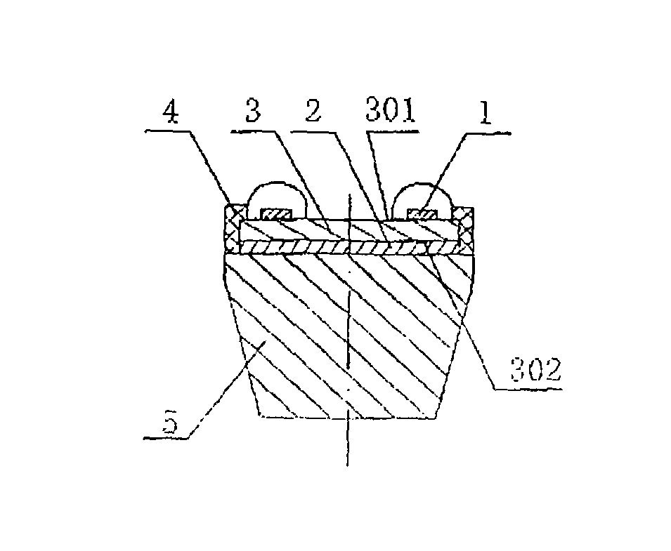
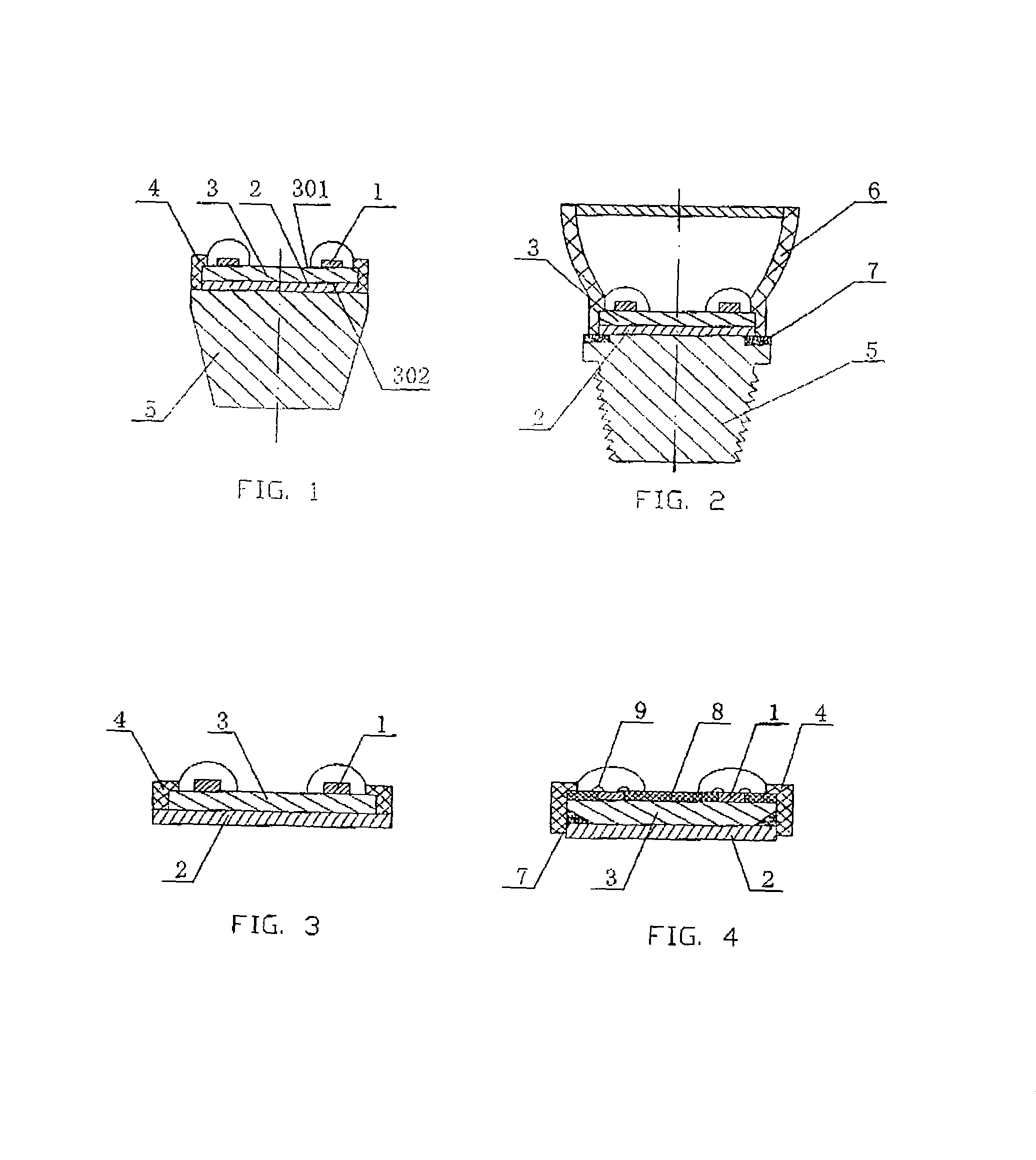
[0030]As shown in FIG. 1, a LED light module of the present invention is illustrated. The thermal conductive core 5 adopts a conical structure. The heat spreading plate 3 adopts a plain panel structure. Two LED wafers are shown in the drawing and are set on Face A 301 of the heat spreading plate 3. When in design, it should be mentioned that the power of a single LED wafer should not be too large and preferably not larger than 2 W. The wafers should be radially and dispersedly arranged on the heat spreading plate. The outer insulator 4 is provided around the peripheral sidewall of the heat spreading plate. The outer insulator 4, which is extended to the high-voltage insulation plate 2 which is set between Face B 302 of the heat dispreading plate 3 and the thermal conductive core 5, together with the high-voltage insulation plate 2 insulate and separate the heat spreading plate 3 from the thermal conductive core 5 and the outer conductor nearby, so as to provide a high-voltage insula...


PUM


Abstract

An LED light module and an LED chip are provided. LED wafers (1) are provided on one side of a heat spreading plate (3) made of copper, aluminum or copper-aluminum composite material with a thickness of more than 0.4 mm and with an area of 5 times of the sum area of the LED wafers larger to reduce the heat-flux density. A high-voltage insulation plate (2) made of a ceramic wafer with a thickness of more than 0.15 mm is provided on the other side of the heat spreading plate (3). The heat spreading plate (3) is separated and insulated by an outer layer insulator (4) with the high-voltage insulation plate (2). This kind design can effectively reduce the internal conduction thermal resistance and raise the insulation strength, and the manufacturing cost can be reduced effectively also.

Description

BACKGROUND OF THE PRESENT INVENTION[0001]1. Field of Invention[0002]The present invention relates to the LED technical field, and more particularly to an LED package structure for reducing the internal heat conduction resistance of an LED light module or an LED chip as well as raising the insulation strength thereof.[0003]2. Description of Related Arts[0004]One of the most important applications of LED technology is the light illumination. The LED light illumination is considered to be the green illumination technology for the next generation of human beings. However, the manufacturing costs of LED illumination products are still high, so that the widely application thereof is hindered. The heat dissipation should be responsible for the high manufacturing costs of LED illumination products. The LED heat dissipating process comprises an internal heat conduction process, and an external heat transfer process of air convection (and / or radiation). The present invention only relates to t...

Claims


Application Information

Patent Timeline
Patent Type & Authority Patents(United States)
IPC IPC(8): F21V29/70F21V25/00F21V29/89F21K99/00F21V29/00
CPCF21V29/70F21K9/00F21V25/00F21V29/89F21Y2101/00F21Y2115/10
Inventor QIN, BIAO
Owner SHENZHEN QIN BO CORE TECH DEV CO LTD
Why Eureka
Try Eureka