Electronic device

a technology of electronic devices and antennas, applied in the structural form of radiating elements, separate antenna unit combinations, resonance antennas, etc., can solve the problems of difficult integration of mobile devices, increased manufacturing complexity and cost, and increased manufacturing costs of multi-band antennas, so as to reduce the effect of metal components

Active Publication Date: 2016-11-29
ASUSTEK COMPUTER INC
View PDF14 Cites 0 Cited by
  • Summary
  • Abstract
  • Description
  • Claims
  • Application Information

AI Technical Summary

Benefits of technology

[0009]The electronic device reduces the effect from the metal components in the mobile device on the antenna, and enables the antenna to operate at more bands.

Problems solved by technology

However, if the dimension of the antenna is large, it is not easy to integrate it to the mobile device.
However, an additional switch or a biasing circuit is needed, which makes the manufacture more complicated and the cost is increased.
Moreover, many components inside or outside the mobile device are made of metal, such as the metal housing, and the radiating loss of the antenna is large due to the electric field concentration, which makes the manufacture of a multiband antenna more difficult.

Method used


Image

  • Electronic device
  • Electronic device
  • Electronic device

Examples


first embodiment

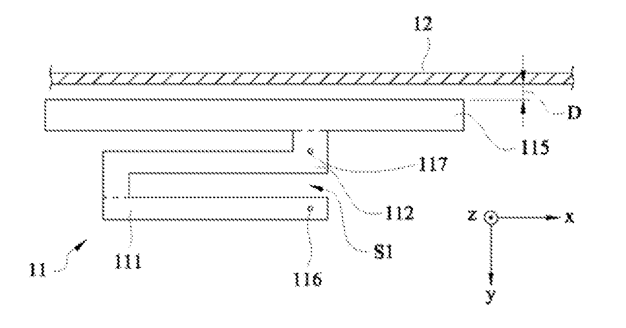
[0036]FIG. 4 is a side view showing an electronic device in the As shown in FIG. 4, the multiband antenna 11 includes a grounding section 111, a feeding section 112 and a radiating element 115. The feeding section 112 includes a feeding point 117 for feeding a signal, and the feeding section 112 is electrically connected to the radiating element 115. The grounding section 111 includes a grounding point 116 connected to the ground, and the grounding section 111 is electrically connected to the feeding section 112. In the following illustration and figures, since the multiband antenna always includes the grounding section, the feeding section and the radiating element, the feeding section includes the feeding point, and the grounding section includes the grounding point, they are omitted in the following, and the symbols can be deduced by analogy.

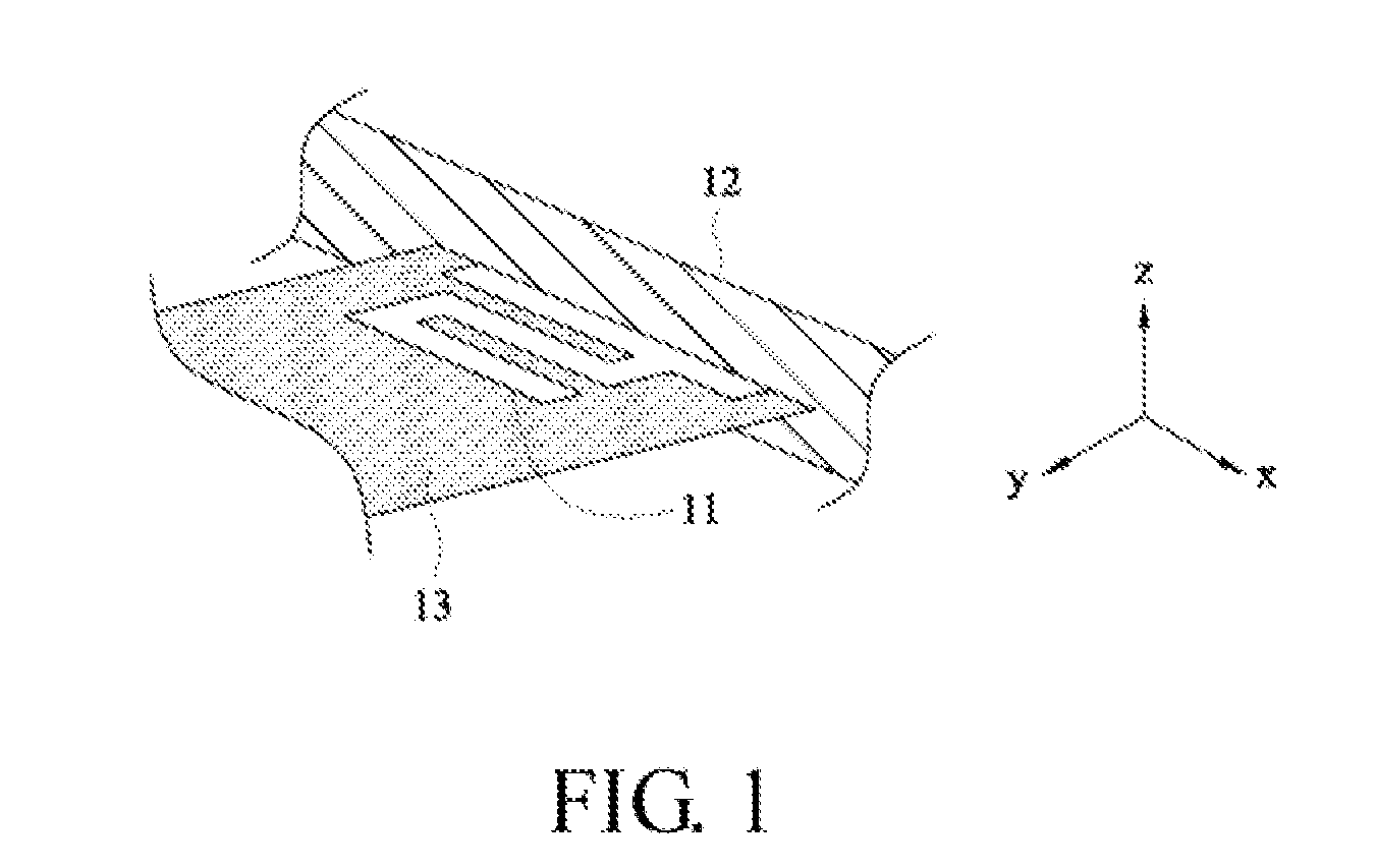
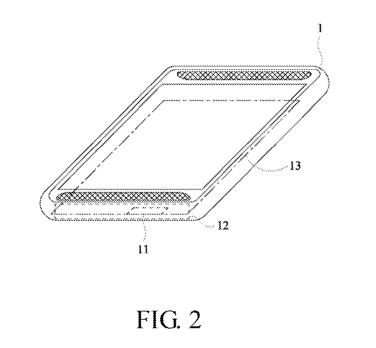
[0037]In the embodiment, when the supporting element 13 is a circuit board of the mobile device 1 (as shown in FIG. 2), the multiband anten...

eleventh embodiment

[0057]FIG. 17 is a side view showing an electronic device in the As shown in FIG. 17, the multiband antenna 16 is disposed at the supporting surface 151 of the supporting element 15. The multiband antenna 16 includes the grounding section 161, the feeding section 162 and the radiating element 165. The grounding section 161 includes a grounding point 166 for connecting the ground. The feeding section 162 is a stepped type element, and includes a feeding point 167 for signals to feed in. A gap is formed between the feeding section 162 and the grounding section 161 and a first slot S2 is formed between the grounding section 161 and the feeding section 162. The length of the first slot S2 can be designed to adjust the impedance of the multiband antenna 16 to conform to a constant value (such as 50 Ω).

[0058]The radiating element 165 is connected to the feeding section 162 and a gap is existed between the radiating element 165 and the conducting element 17. A second slot S3 is formed bet...


PUM


Abstract

An electronic device includes a conducting element, a supporting element, and a multiband antenna is disclosed. The conducting element is connected to the ground of the electronic device by a high impedance connection. The supporting element has a supporting surface, and the supporting surface and the conducting element are perpendicular. The multiband antenna is disposed at the supporting surface and includes a radiating element, and the radiating element and the conducting element form a coupling capacitor.

Description

CROSS-REFERENCE TO RELATED APPLICATION[0001]This application claims the priority benefits of U.S. provisional application Ser. No. 61 / 843,455, filed on Jul. 8, 2013 and Taiwan application serial No. 102140779, filed on Nov. 8, 2013. The entirety of the above-mentioned patent applications are hereby incorporated by references herein and made a part of specification.BACKGROUND OF THE INVENTION[0002]1. Field of the Invention[0003]The invention relates to an electronic device and, more particularly, to an electronic device with an antenna.[0004]2. Description of the Related Art[0005]In wireless communication, a mobile device usually needs a competent transceiver system to maintain the two-way communication quality between the mobile device and the base station. A dipole antenna and a monopole antenna are usually disposed at the external surface of the mobile device or integrated to the mobile device. Another type of antenna used commonly is a planar inverted F antenna (PIFA), and the FI...

Claims


Application Information

Patent Timeline
Patent Type & Authority Patents(United States)
IPC IPC(8): H01Q1/38H01Q9/04H01Q1/24H01Q5/371
CPCH01Q9/0421H01Q1/243H01Q1/38H01Q5/371H01Q1/521H01Q21/30
Inventor HSIEH, WANG-TAHUANG, CHUAN-CHIENYEH, KUEI-SHUNSHIH, WEI-HSINLIANG, CHIH-CHAN
Owner ASUSTEK COMPUTER INC
Why Eureka
Try Eureka