Low-temperature epitaxial method for manufacturing backside field stop layer of insulated gate bipolar transistor (IGBT)
- Summary
- Abstract
- Description
- Claims
- Application Information
AI Technical Summary
Benefits of technology
Problems solved by technology
Method used
Image

Examples
Embodiment Construction
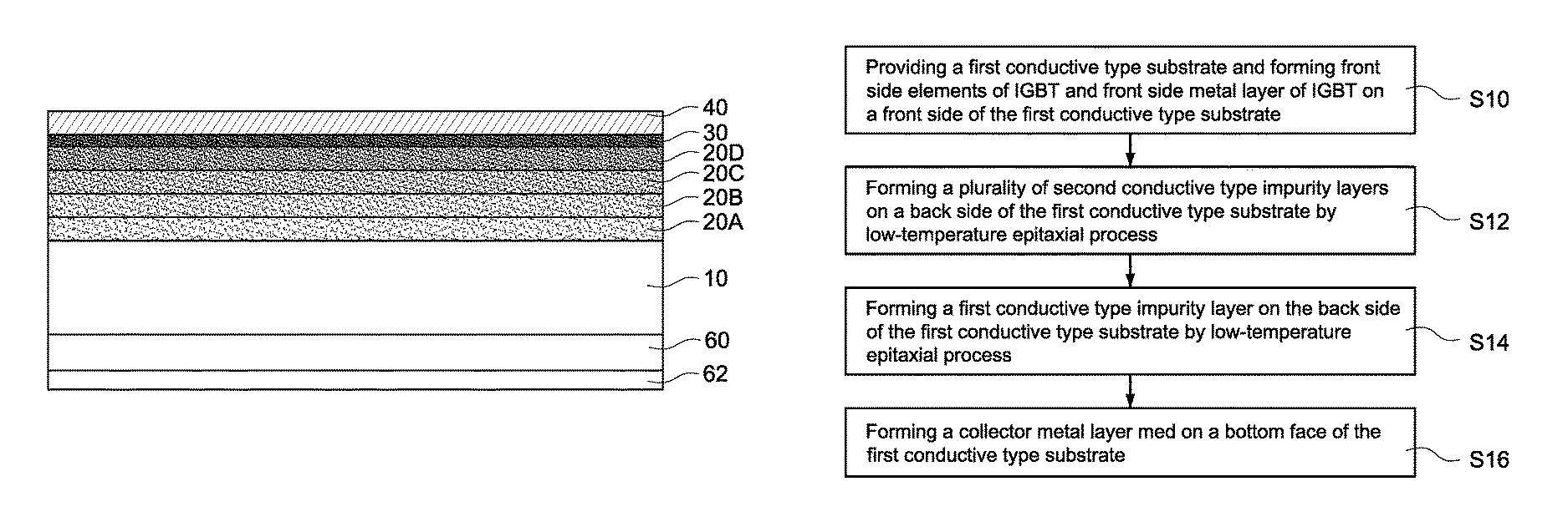
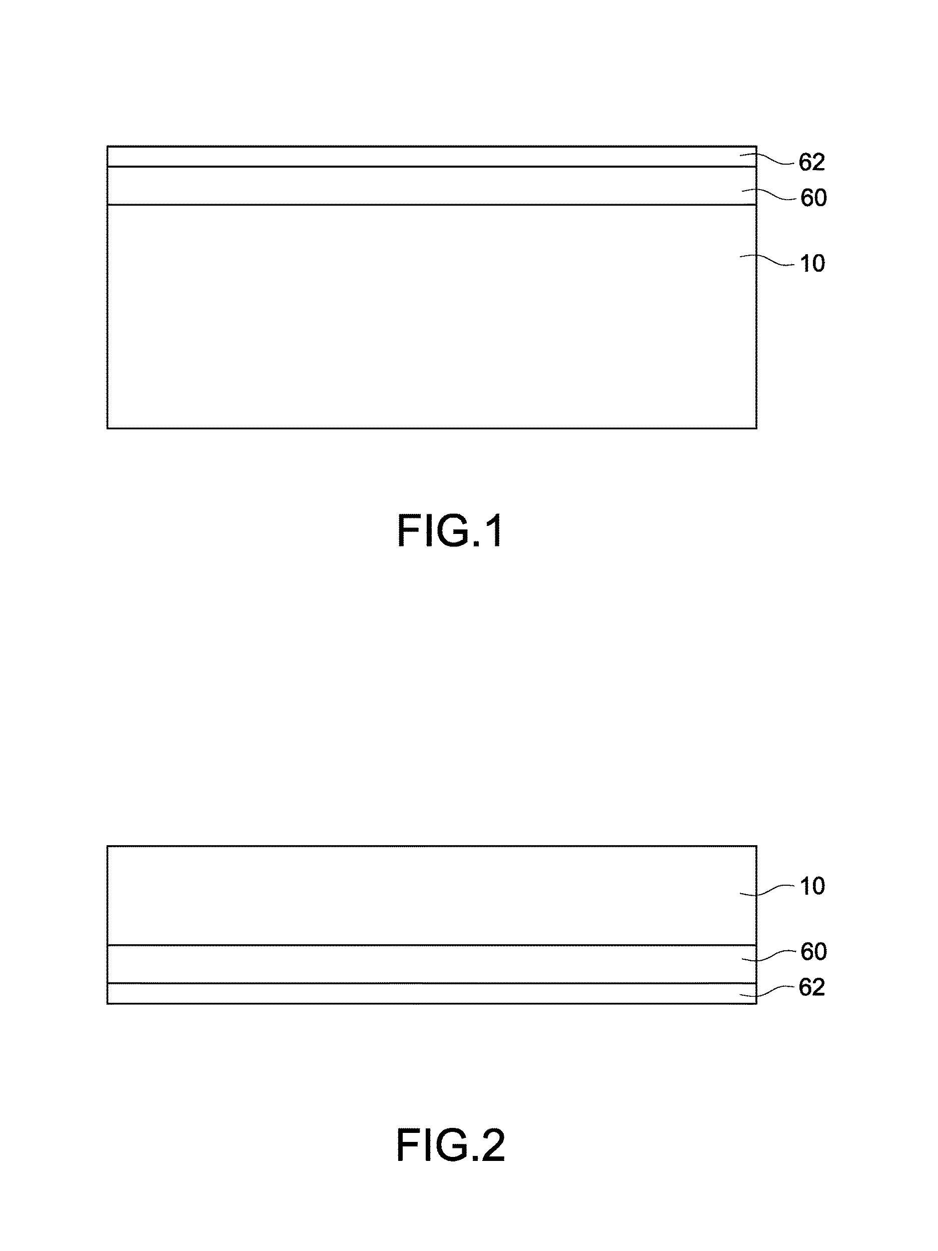
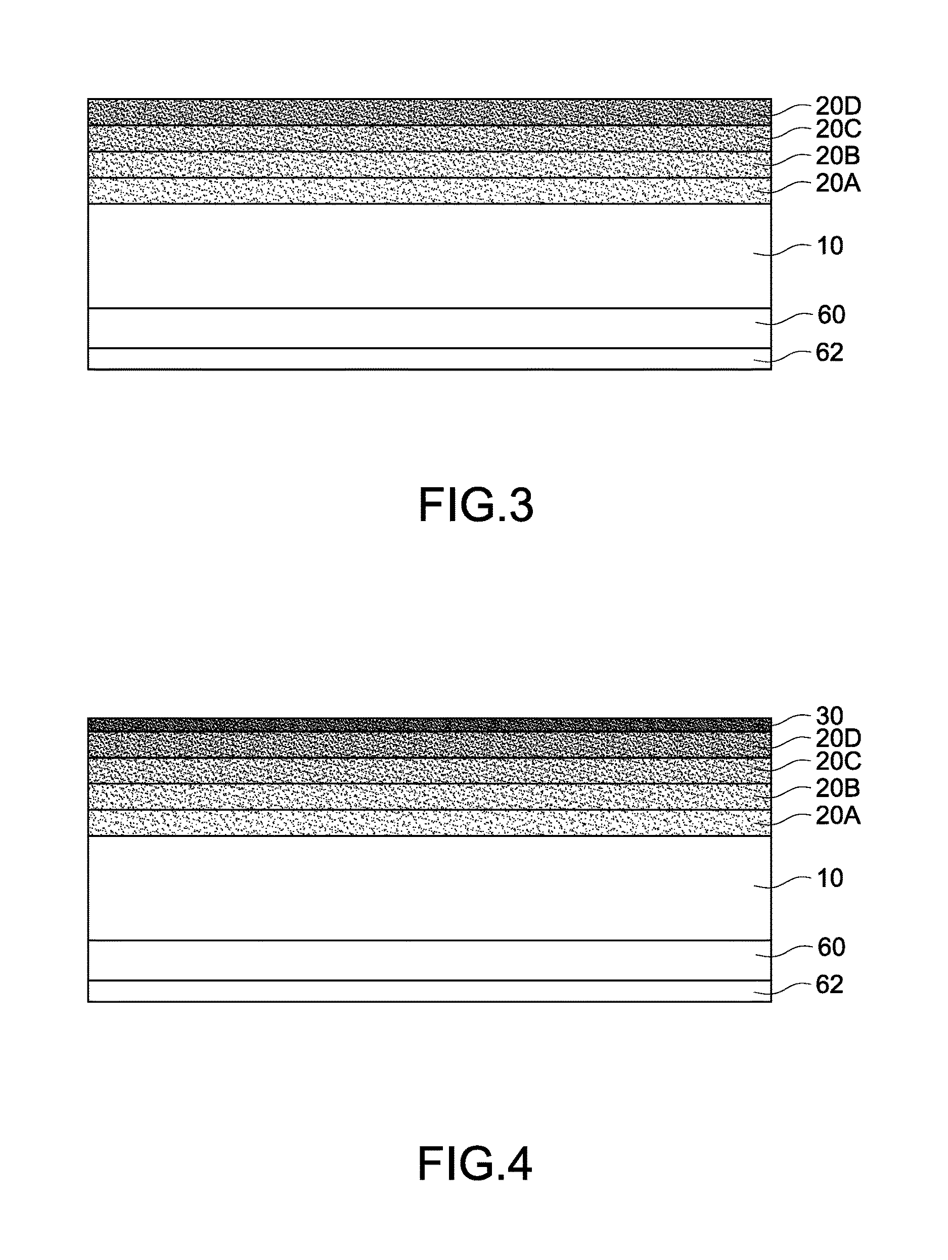
[0015]FIGS. 1 to 5 are sectional views showing the steps of low-temperature epitaxial method for manufacturing backside field stop layer of insulated gate bipolar transistor (IGBT) according to an embodiment of the present invention. With also reference to FIG. 6, this figure shows the flowchart of low-temperature epitaxial method for manufacturing backside field stop layer of IGBT according to an embodiment of the present invention. As shown in FIG. 6, the low-temperature epitaxial method for manufacturing backside field stop layer of IGBT comprises following steps: (S10) providing a first conductive type substrate and forming front side elements of IGBT and front side metal layer of IGBT on a front side of the first conductive type substrate; (S12) forming a plurality of second conductive type impurity layers on a back side of the first conductive type substrate by low-temperature epitaxial process; (S14) forming a first conductive type impurity layer on the back side of the first...
PUM
 Abstract
Description
Claims
Application Information
 - R&D Engineer
- R&D Manager
- IP Professional
- Industry Leading Data Capabilities
- Powerful AI technology
- Patent DNA Extraction
Browse by: Latest US Patents, China's latest patents, Technical Efficacy Thesaurus, Application Domain, Technology Topic.
© 2024 PatSnap. All rights reserved.Legal|Privacy policy|Modern Slavery Act Transparency Statement|Sitemap