Biosensor array formed by junctions of functionalized electrodes
- Summary
- Abstract
- Description
- Claims
- Application Information
AI Technical Summary
Benefits of technology
Problems solved by technology
Method used
Image
Examples
first preferred embodiment
Woven Network of Conductors—from the Array Assembly to the Measurement
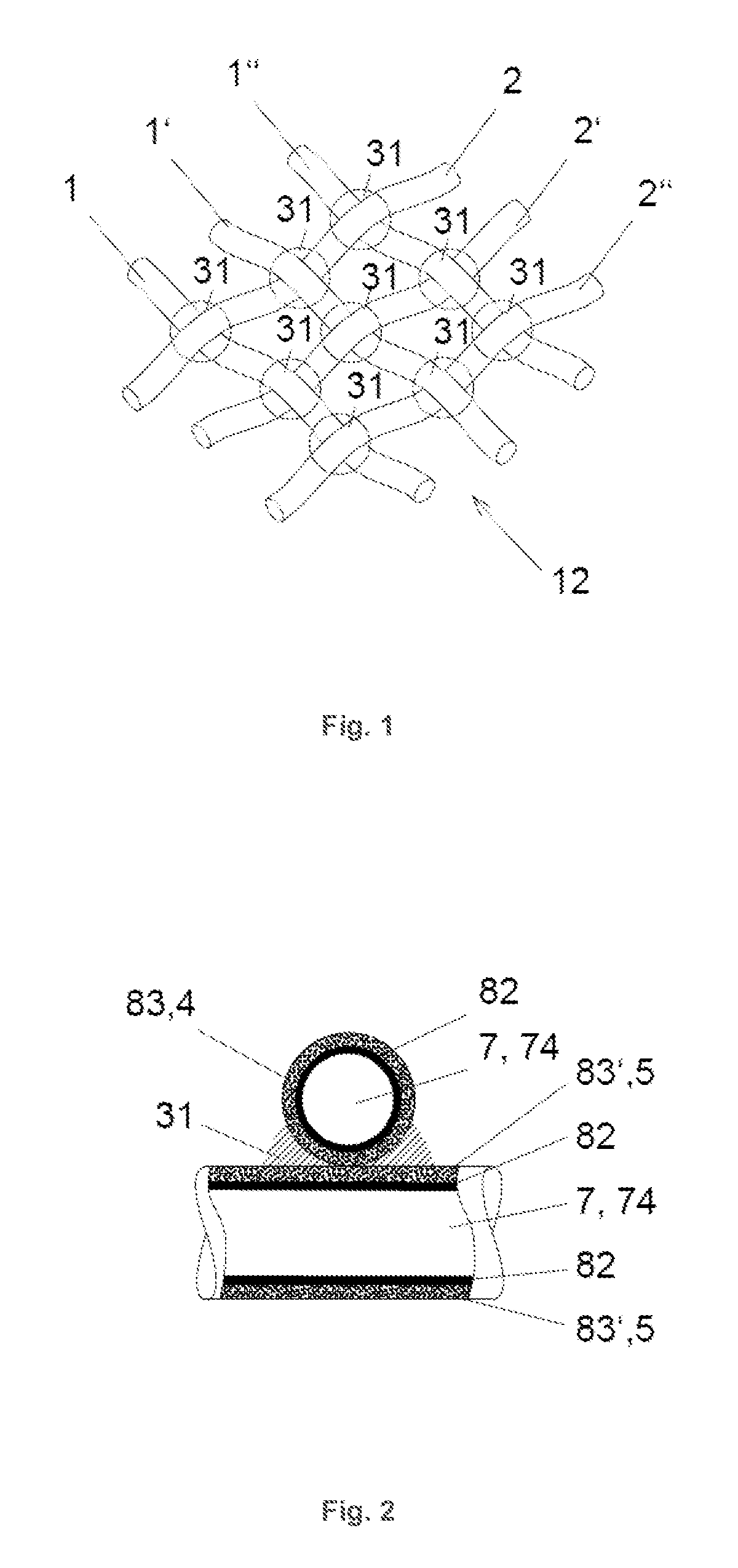
[0123]The first preferred embodiment of the invention, which is shown in FIG. 1, describes a sensor array 12 with woven sensor half elements 1, 2, which are grouped as row elements 1 and column elements 2. One group of unidirectional sensor half elements 1, 2 is denoted as row elements 1. The remaining sensor half elements 1, 2 are referred to as column elements 2. Together, the sensor half elements 1, 2 are assembled in a weave-like or woven structure. Accordingly, each row element 1 intersects or crosses or approaches or touches each column element 2 in exactly one junction area 31. The number of junction areas 31 within one sensor array 12 equals to the product of the number of row elements 1 and column elements 2.
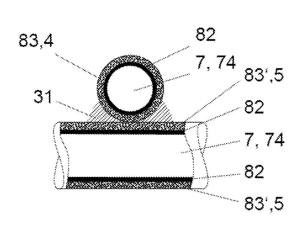
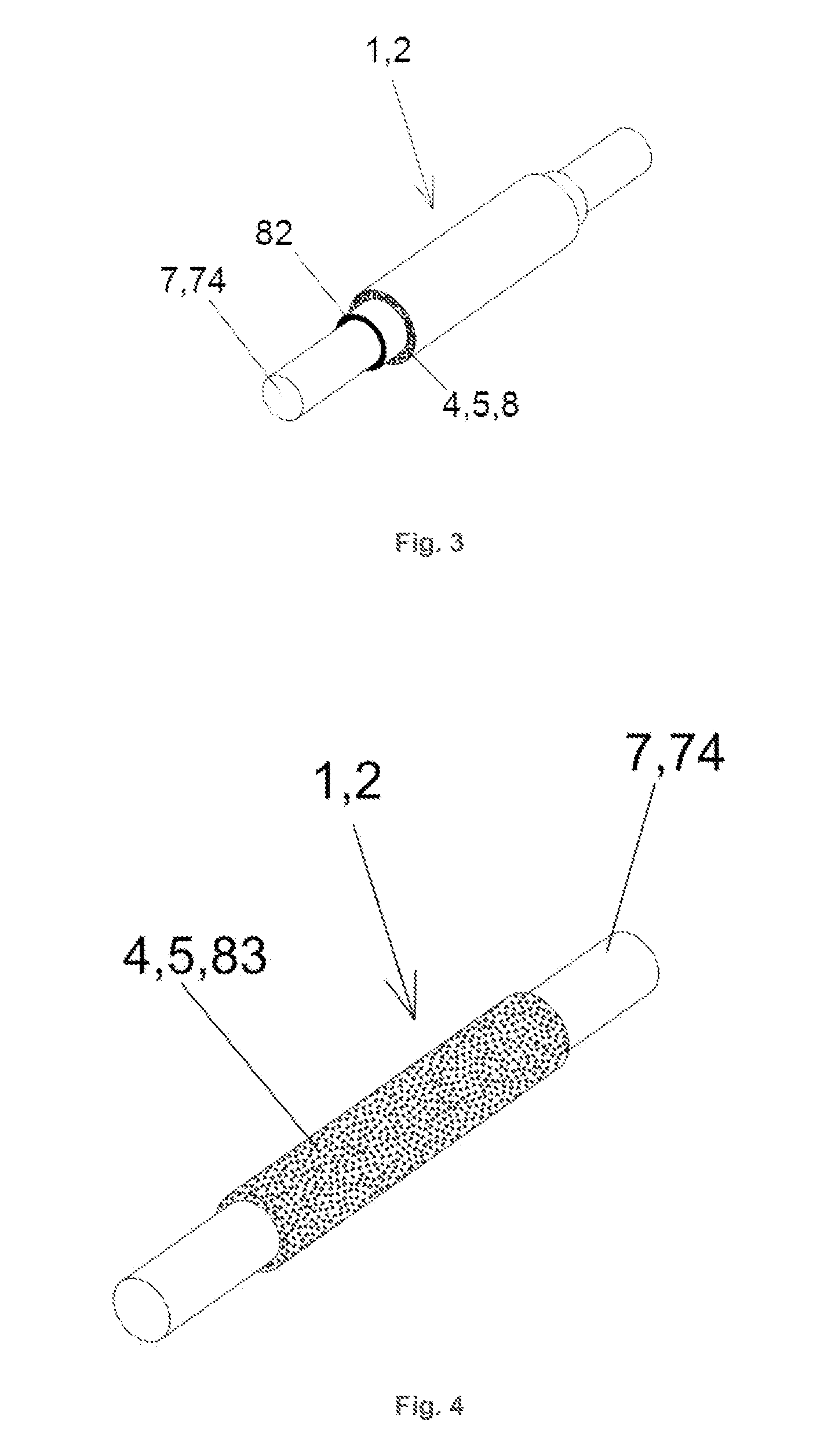
[0124]The present example contains linear sensor half elements 1, 2 as shown in FIG. 2. The carrier 7 is an elongated conductor 74 and has a convex almost circular cross-section. The cross section of ...
second preferred embodiment
Sensor Arrays with Common Carrier Plates
[0207]The second preferred embodiment describes structures which are fabricated through arranging and aligning sensor half elements 1, 2 on one of two common carriers 61, 62 as shown in FIG. 14.
[0208]The sensor half elements 1, 2 are functionalized according to the method of functionalization as described above. Each of the row elements 1 is arranged and aligned on the first common carrier 61, each of the column elements 2 is arranged and aligned on the second common carrier. The sensor half elements 1, 2 are supported by the respective common carrier 61, 62. In this preferred embodiment of the invention, the row elements 1 are arranged in parallel on the first common carrier 61 and the column elements 2 are arranged in parallel on the second common carrier 62. One of the common carriers 61, 62 is depicted in FIG. 15. The row elements 1 and the column elements 2 are aligned perpendicular to each other. The parts of the surface of the row eleme...
PUM
| Property | Measurement | Unit |
|---|---|---|
| dielectric constant | aaaaa | aaaaa |
| dielectric constant | aaaaa | aaaaa |
| length | aaaaa | aaaaa |
Abstract
Description
Claims
Application Information


