LED metal substrate package and method of manufacturing same

a technology of metal substrate and packaging, which is applied in the direction of basic electric elements, electrical apparatus, and semiconductor devices, can solve the problems of shortening the lifetime, generating thermal resistance, and aging of characteristics, and achieves excellent heat radiation and bonding properties, improved heat radiation properties, and improved efficiency and the effect of the lifetime of the optical device chip

Active Publication Date: 2017-01-31
POINT ENG
View PDF10 Cites 2 Cited by
  • Summary
  • Abstract
  • Description
  • Claims
  • Application Information

AI Technical Summary

Benefits of technology

[0032]According to an exemplary embodiment of the present invention as described above, an electrode layer is formed on a portion of a metal package comprising aluminum, then an optical device chip is bonded on said electrode layer using a gold-tin (Au / Sn) alloy soldering layer having excellent heat radiation and bonding properties so that the package has a better heat radiation property than the LED metal package using a conventional silver (Ag) epoxy, as a result, it has an effect that the efficiency and the lifetime of the optical device chip can be increased. Especially the UV LEDs radiate more heat than the visible LEDs, however, as described in the exemplary embodiments of the present invention, by applying gold-tin (Au / Sn) soldering to the metal package substrate comprising aluminum, the heat radiation property of the optical device chip is enhanced, so that an enhancement effect on the efficiency and the lifetime of an UV LED can be expected.

Problems solved by technology

That is, in a high efficiency LED, high temperature heat is produced, therefore this heat must be radiated effectively otherwise temperature rising on the LEDs causes ageing of the characteristics thereby shortening the lifetime.
For an optical device having an above described structure, a silver epoxy has a good electrical conductivity and bonding property, however, the relatively low heat conductivity thereof generates a thermal resistance in a package wherein a high power optical device is mounted.
Moreover, the foresaid problem will be more significant if the optical device chip 40 is an UV optical device which generates more heat compared to an optical device for a visible light region.

Method used


Image

  • LED metal substrate package and method of manufacturing same
  • LED metal substrate package and method of manufacturing same
  • LED metal substrate package and method of manufacturing same

Examples


Embodiment Construction

[0041]Hereinafter, a preferred exemplary embodiment of the present invention will be described in detail with reference to the accompanying drawings. In describing the present invention, the detailed description will be omitted when determined that detailed descriptions about: related publicly known functions or configurations, manufacturing process of a metal substrate wherein a vertical insulation layer is formed, and packing processes after the electrode wire bonding of an optical device chip, and the like may obscure the gist of the present invention.

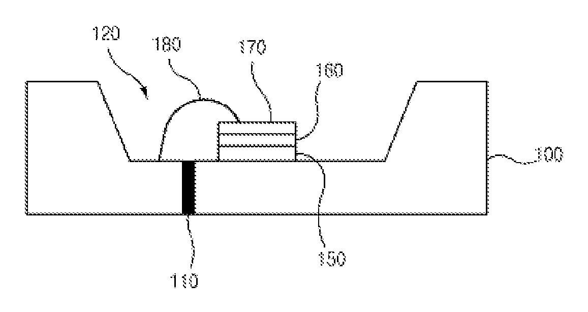
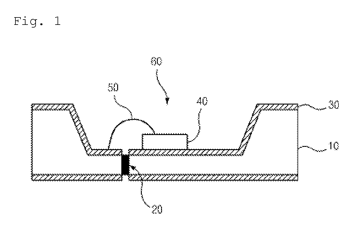
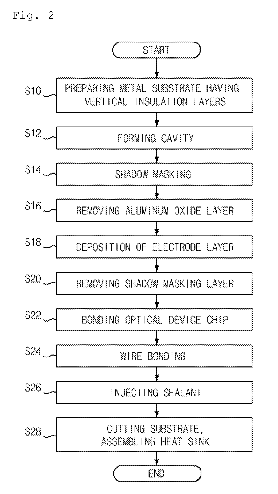
[0042]First, FIG. 2 is a manufacturing process flow diagram of an LED metal substrate package according to an exemplary embodiment of the present invention, and FIGS. 3a to 3g are the exemplary illustrations of the cross-sectional views at each corresponding process step of an LED metal substrate package being manufactured according to FIG. 2. FIG. 4 is an exemplary illustration of a cross-sectional view of an LED metal substrate pa...


PUM


Abstract

The present invention relates to an LED metal substrate package, and particularly, to an LED metal substrate package having a heat dissipating structure, and a method of manufacturing same. The method comprises at least the steps of: forming at least one cavity having a groove of a predetermined depth in a metal substrate that is electrically separated by at least one vertical insulation layer, the cavity having one vertical insulation layer built in a floor thereof; treating all surfaces, except portions of the top surface of the metal substrate formed in the respective cavities, with shadow masking; removing an oxide film formed on the surface portions that have not been treated with masking; depositing an electrode layer on each of the surface portions of the oxide layer that have been removed; removing the shadow mask; performing Au / Sn soldering on the electrode layer and bonding an optical device chip; and wire bonding one electrode of the optical device, disposed on one side of the metal substrate with respect to each of the vertical insulation layers, through wires to the metal substrate disposed on the other side of each of the vertical insulation layers. The present invention forms solder using Au / Sn material, which has good heat dissipating characteristics and good bonding characteristics, on the electrode layer to bond an optical device chip, so as to have excellent heat dissipating performance compared to existing LED metal packages that use Ag epoxy.

Description

TECHNICAL FIELD[0001]The present invention relates to an LED metal substrate package, more particularly to an LED metal substrate package having a heat radiating structure and a method for manufacturing same.BACKGROUND ART[0002]Semiconductor light emitting diode (LED) is receiving attention from various fields as an environment friendly light source. Recently, as applications of LEDs are expanding to various fields such as interior and exterior illuminations, automobile headlights, and back-light units (BLU) of display devices, there are needs for high optical efficiency and excellent heat radiation characteristics. For high efficiency LEDs, materials or structures of the LEDs should be improved primarily, however there is a need for improvement in the structures of the LED packages and the materials used therein.[0003]That is, in a high efficiency LED, high temperature heat is produced, therefore this heat must be radiated effectively otherwise temperature rising on the LEDs causes...

Claims


Application Information

Patent Timeline
Patent Type & Authority Patents(United States)
IPC IPC(8): H01L33/62H01L33/48
CPCH01L33/62H01L33/486H01L2224/13H01L2224/48091H01L2224/73265H01L2933/0033H01L2933/0066H01L2924/00014H01L33/48H01L33/38H01L2933/0016
Inventor AHN, BUM MOPARK, SEUNG HO
Owner POINT ENG
Why Eureka
Try Eureka