Light emitting module, a lamp, a luminaire and a display device

a technology of light emitting modules and luminaires, applied in semiconductor devices, light source combinations, lighting and heating apparatus, etc., can solve the problems of poor recycling efficiency of light directed back from the luminescent layer to the led, inefficiency of light trapped inside the light emitting device, so as to reduce the cost level of the display device

Active Publication Date: 2017-03-21
LUMILEDS
View PDF33 Cites 15 Cited by
  • Summary
  • Abstract
  • Description
  • Claims
  • Application Information

AI Technical Summary

Benefits of technology

[0015]The value of the base reflection coefficient is at least larger than the value of the solid state light emitter reflection coefficient and consequently the base absorbs less light than the solid state emitter. This is advantageous because more light is reflected by the base and therefore more light may be emitted through the light exit window in the ambient of the light emitting module. It actually means that more light is reflected by the base which is subsequently recycled instead of absorbed. The efficiency of the light emitting module as a whole improves, as light losses in the light emitting module according to the invention are minimized. Compared to light emitting modules with a luminescent layer directly on top of the solid state light emitter, less light is lost by the light absorption of the solid state light emitter. Compared to light emitting modules with a remote luminescent layer acting as a partially diffusive reflective layer, the light that is reflected, back scattered and / or re-emitted by the partially diffusive reflective layer to the inside of the module is recycled more efficiently as it has less interaction (reflections) inside the module before exiting the light exit window. As a result, a light emitting module according to the invention is relatively efficient.
[0055]The lamp, luminaire and the display device according to, respectively, the second, third and fourth aspect of the invention provide the same benefits as the light emitting module according to the first aspect of the invention and have similar embodiments with similar effects as the corresponding embodiments of the light emitting module.

Problems solved by technology

Especially the absorption of light results in an inefficiency of the light emitting device.
A problem of the light emitting modules with the light emitters which have the luminescent layer directly on top is that light directed back from the luminescent layer to the LED suffers from poor recycling efficiency due to the fact that back reflectors inside the LED have a limited reflectance (typically the back mirror is silver, with 90% reflectance levels).
In reality the actual reflectance is even lower as the light emitter material, typically GaN / InGaN or AlInGaN, has a high refractive index, causing light to be trapped inside the light emitter and thus further limiting metal reflectance.
Another problem of these light emitting modules is the formation of hot spots in which most of the light is concentrated in the area on top of the LED and the light output of the module is therefore highly non-uniform resulting in hot spots both in light output and thermal distribution.
Furthermore, a phosphor layer on top of the LED die may get relatively hot and is excited with a high flux density, leading to a non-optimal phosphor conversion efficiency thereby limiting the luminescent performance.
The relatively bulky remote luminescent layer solutions cannot be used in size constrained applications, such as spot lamp applications, for example halogen replacement lamps and parabolic reflector lamps.
Another disadvantage of light emitting modules with a remote luminescent layers is that the relatively large area of the luminescent layer results in relatively high material cost levels.
In addition, the heat conductance within the phosphor layer is only directed laterally towards the side walls of the light emitter and due to their bulky construction, the ability to direct the heat away from the remote phosphor plate is limited.

Method used


Image

  • Light emitting module, a lamp, a luminaire and a display device
  • Light emitting module, a lamp, a luminaire and a display device
  • Light emitting module, a lamp, a luminaire and a display device

Examples


Embodiment Construction

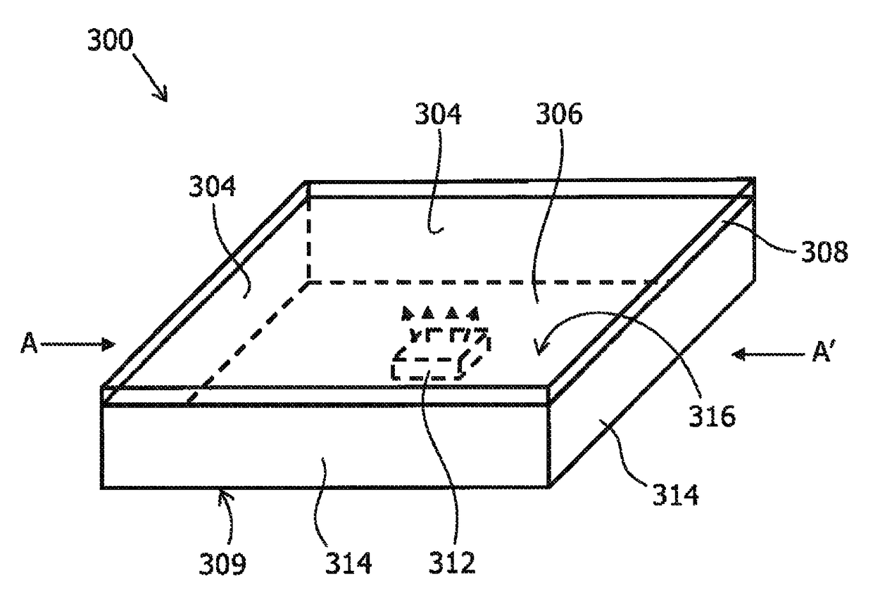
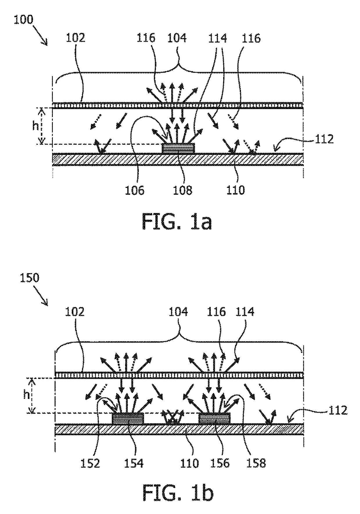
[0087]A first embodiment is shown in FIG. 1a which shows a cross-section of a light emitting module 100 according to the first aspect of the invention. The light emitting module 100 has a light exit window 104. The light exit window 104 in this embodiment is formed by a luminescent layer 102 which comprises luminescent material. The luminescent material converts at least a part of light of a first color range 114 which impinges on the luminescent material into light of a second color range 116. At another side of the light emitting module 100 a base 110 is provided which has a light reflecting surface 112 that faces towards the light exit window 104. On the base 110 a solid state light emitter 108 is provided which emits, in use, light of the first color range 114 towards a part of the light exit window 104. The base is typically provided with electrode structures to contact the dies or plurality of dies of the solid state light emitter 108 to provide electrical power. The electrode...


PUM


Abstract

A light emitting module includes at least one LED mounted on a reflective base and surrounded by reflective walls to form a cavity. A partially diffusive layer containing a phosphor is mounted above the LED with a gap therebetween. Some of the light emitted by the phosphor is backscattered toward the LED, base, and walls. The LED absorbs a significant amount of the light, while the reflective base and walls efficiently reflect over 90% of the light back toward the phosphor layer for exiting the module. Various equations are provided that allow the designer to select an optimal gap between the LED and the partially diffusive layer to maximize light extraction efficiency out of the diffusive layer. The optimal gap range for maximizing light extraction efficiency is a product of LED largest linear length, LED surface area, base area, wall area, and reflective coefficients of the various elements.

Description

CROSS-REFERENCE TO PRIOR APPLICATIONS[0001]This application is the U.S. National Phase application under 35 U.S.C. §371 of International Application No. PCT / IB2012 / 051405, filed on Mar. 23, 2012, which claims the benefit of EP 11181914.0 Sept. 20, 2011. These applications are hereby incorporated by reference.FIELD OF THE INVENTION[0002]The invention relates to a light emitting module which comprises a luminescent layer and a solid state light emitter. The invention further relates to a lamp, a luminaire and a display device comprising a light emitting module.BACKGROUND OF THE INVENTION[0003]Published patent application US2009 / 0322208A1 discloses a light emitting device. A Light Emitting Diode (LED) is provided within a conical cavity formed by a recessed housing. At the front side of the recessed housing the conical cavity is covered with a transparent thermal conductor layer on which a refractory luminescent layer is provided. At the backplane of the recessed housing a heat sink is...

Claims


Application Information

Patent Timeline
Patent Type & Authority Patents(United States)
IPC IPC(8): F21V9/00F21K9/64F21K9/62H01L33/00H01L33/50H01L33/60F21K99/00F21V9/40F21Y113/13F21Y115/10
CPCF21K9/62F21K9/64H01L33/507H01L33/60F21Y2113/13F21Y2115/10H01L2924/0002H01L2933/0091H01L2924/00
Inventor JAGT, HENDRIK JOHANNES BOUDEWIJNVDOVIN, OLEXANDR VELENTYNOVYCHVERSCHUREN, COEN ADRIANUSDIJKEN, DURANDUS KORNELIUSKLEIJNEN, CHRISTIANKRIJN, MARCELLINUS PETRUS CAROLUS MICHAEL
Owner LUMILEDS
Why Eureka
Try Eureka