Circuit board and manufacturing method thereof

a technology of circuit board and manufacturing method, applied in the field of circuit board, can solve the problems of challenging to completely fill a region on a portion of the dielectric substrate, and achieve the effect of high reliability

Active Publication Date: 2017-04-25
UNIMICRON TECH CORP
View PDF3 Cites 12 Cited by
  • Summary
  • Abstract
  • Description
  • Claims
  • Application Information

AI Technical Summary

Benefits of technology

[0006]The invention provides a circu

Problems solved by technology

However, when the circuit pattern in the circuit board requires a greater thickness (e.g., when the circuit board is applied in a device for vehicles), it is usually challenging to completely fill a region on a portion of the dielectric substrate exposed by the circuit pa

Method used


Image

  • Circuit board and manufacturing method thereof
  • Circuit board and manufacturing method thereof
  • Circuit board and manufacturing method thereof

Examples


first embodiment

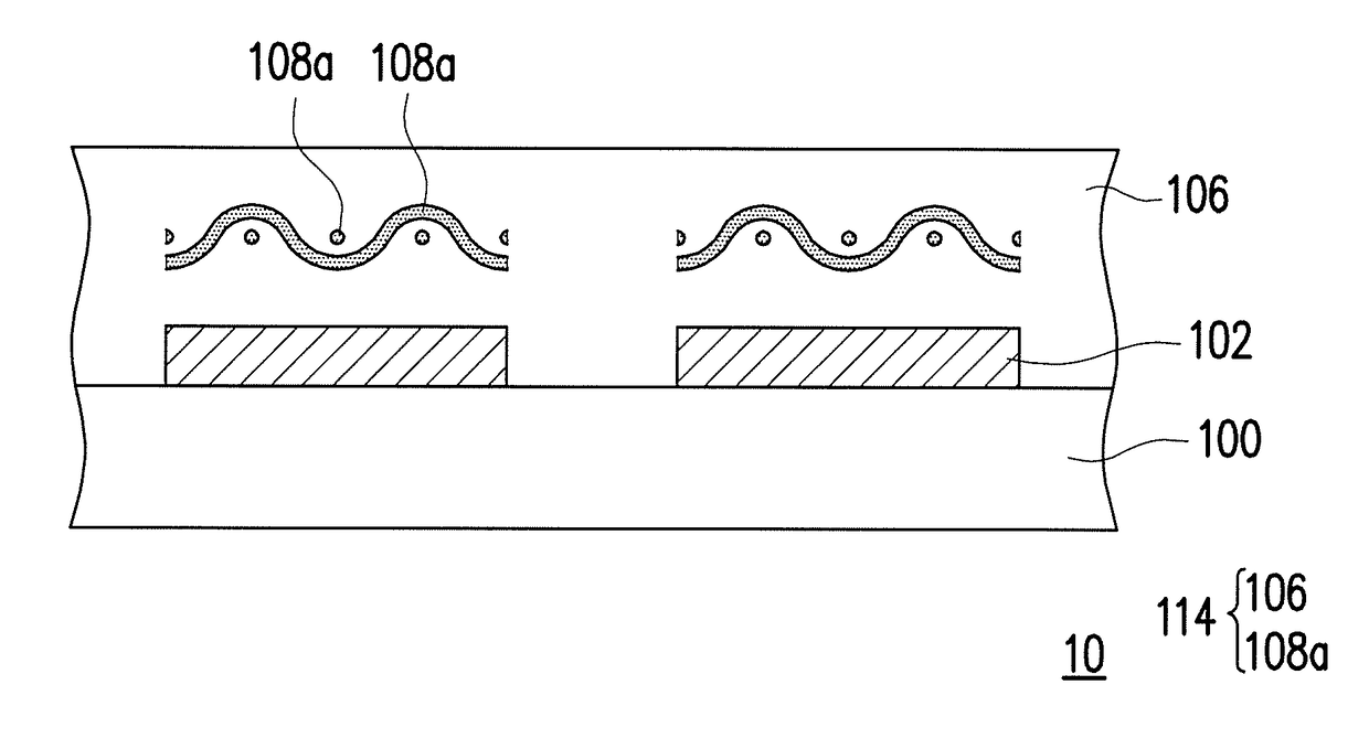
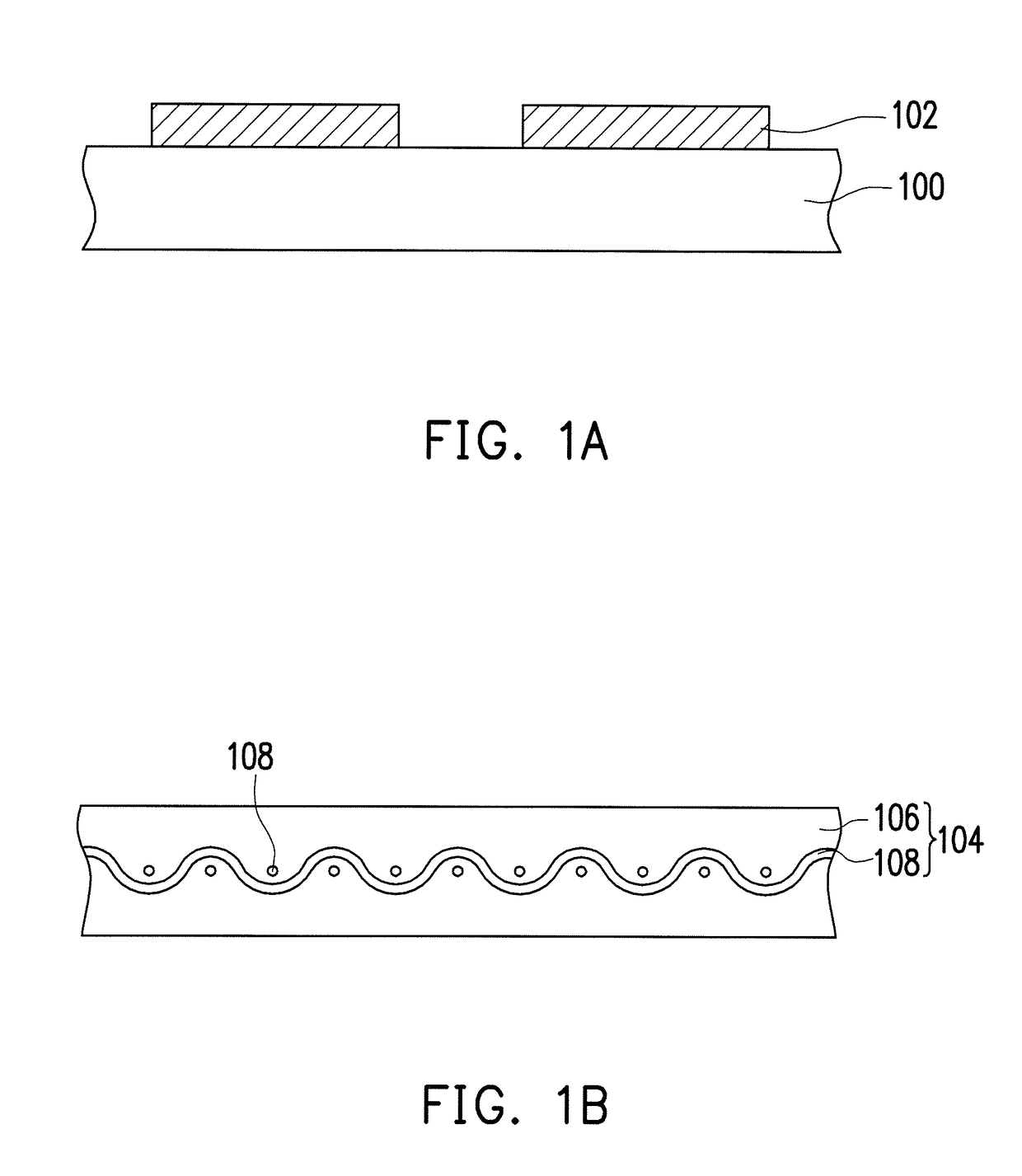
[0025]FIGS. 1A to 1D are schematic cross-sectional view illustrating a manufacturing process of a circuit board according to a first embodiment of the invention. First of all, referring to FIG. 1A, a circuit pattern 102 is formed on a dielectric substrate 100. The circuit pattern 102 exposes a portion of the dielectric substrate 100. A process of forming the circuit pattern 102 includes, for example, forming a conductive material layer on the dielectric substrate 100 by compression and patterning the conductive material layer. A material of the dielectric substrate 100 includes epoxy resin, glass fiber cloth, or ceramics. In this embodiment, a thickness of the circuit pattern 102 is greater than 50 μm. When the thickness of the circuit pattern 102 is greater than 50 μm, the circuit board formed accordingly is suitable for a device for vehicles requiring a higher current. However, it should be noted that the invention is not limited thereto.

[0026]Then, referring to FIG. 1B, a dielect...

second embodiment

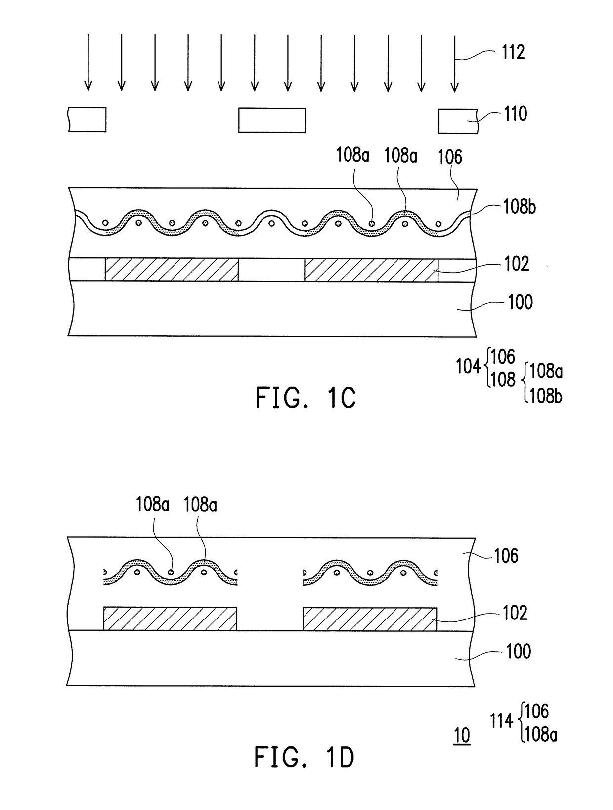
[0031]FIGS. 3A to 3C are schematic cross-sectional view illustrating a manufacturing process of a circuit board according to a second embodiment of the invention. In this embodiment, components and steps identical to those of the first embodiment will not be further reiterated. First of all, referring to FIG. 3A, before disposing the dielectric layer 104 on the dielectric substrate 100, the selective exposing process is performed to the dielectric layer 104 by using the photomask 110. When the light beam 112 passes through the photomask 110 and irradiates the dielectric layer 104, the portion 108a having a higher glass transition temperature and the portion 108b remaining at the original glass transition temperature are formed in the photosensitive mesh-shaped fiber 108, as illustrated in FIG. 1C. Since the photomask 100 has the opening corresponding to the position of the circuit pattern 102, the portion 108a having the higher glass transition temperature formed herein may correspo...


PUM

PropertyMeasurementUnit
Thicknessaaaaaaaaaa
Dielectric polarization enthalpyaaaaaaaaaa
Glass transition temperatureaaaaaaaaaa

Abstract

A circuit board and a manufacturing method thereof are provided. The circuit board includes a dielectric substrate, a circuit pattern and a dielectric layer. The circuit pattern is disposed on the dielectric substrate. The dielectric layer is disposed on the dielectric substrate and covers the circuit pattern. The dielectric layer includes a dielectric matrix and a mesh-shaped fiber structure disposed in the dielectric matrix. There is no mesh-shaped fiber structure on a portion of the dielectric substrate exposed by the circuit pattern.

Description

BACKGROUND OF THE INVENTION[0001]1. Field of the Invention[0002]The invention relates to a circuit board and a manufacturing method thereof, and particularly relates to a circuit board where there is no mesh-shaped fiber structure in a dielectric layer on a portion of a dielectric substrate exposed by a circuit pattern and a manufacturing method thereof.[0003]2. Description of Related Art[0004]Generally speaking, a manufacturing process of a circuit board includes steps such as forming a circuit pattern on a substrate, forming a dielectric layer covering the circuit pattern, forming a conductive via in the dielectric layer, and forming another layer of circuit pattern on the dielectric layer, etc. The dielectric layer is usually formed of a resin matrix and a mesh-shaped glass fiber structure in the resin matrix. In the step of forming the dielectric layer covering the circuit pattern, the dielectric layer is usually disposed on the substrate where the circuit pattern is already for...

Claims


Application Information

Patent Timeline
IPC IPC(8): H05K1/03H05K3/00
CPCH05K1/0366H05K3/0023H05K2203/1105H05K3/4673H05K2201/0278H05K2201/029H05K2203/0557
Inventor CHEN, YIN-JUCHANG, CHI-MINYU, CHENG-PO
Owner UNIMICRON TECH CORP
Why Eureka
Try Eureka