Analog delay cell and tapped delay line comprising the analog delay cell

a delay cell and analog technology, applied in the field of electronic circuits, can solve the problems of long delay lines and large dimension components, insufficient bandwidth, and many segments,

Inactive Publication Date: 2017-05-16
NXP USA INC
View PDF87 Cites 26 Cited by
  • Summary
  • Abstract
  • Description
  • Claims
  • Application Information

AI Technical Summary

Problems solved by technology

However, the transmission lines may require long lines and large dimension components to implement.
Also, the resulting bandwidth may be too narrow and need many segments for high speed SerDes (serializer / deserializer) applications.
Conventional active analog delay cells with active inductors may require further inductance compensation circuits, and it may be difficult to maintain the consistency of the delay lines.
In addition, an active inductor may have its own bandwidth limitations.
Prior digital-based delay cells, for example, D-type flip-flops, or latches, may not be able to support the required high speed capacity at data rates greater than about 10 gigabits per second (Gb / s).
Also, digital-based delay cells may not be able to support small input data amplitudes due to intersymbol interference (ISI).

Method used


Image

  • Analog delay cell and tapped delay line comprising the analog delay cell
  • Analog delay cell and tapped delay line comprising the analog delay cell
  • Analog delay cell and tapped delay line comprising the analog delay cell

Examples


Embodiment Construction

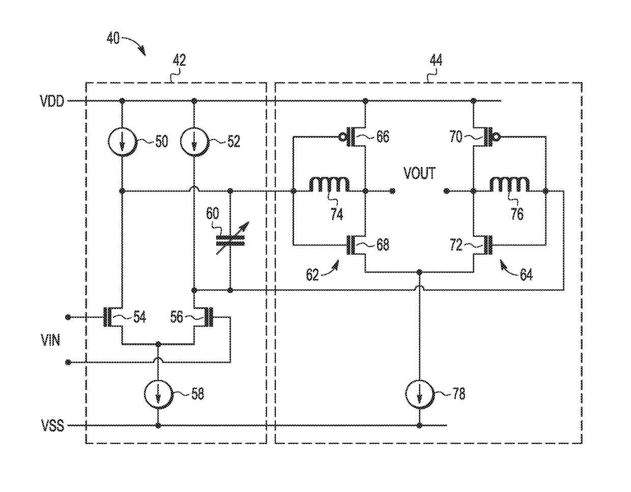
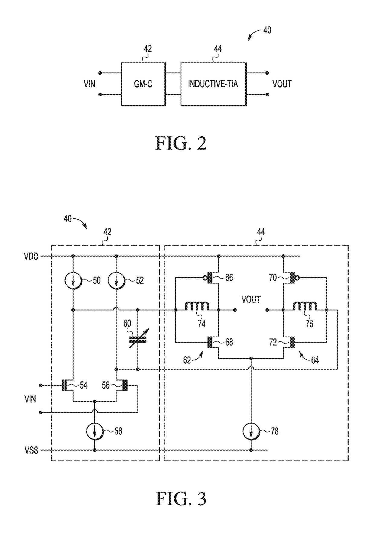
[0018]Generally, there is provided, an analog delay cell with a transconductance-capacitance stage and an inductive transimpedance amplifier stage that provides an all-pass transfer function. In another embodiment, an adaptive analog delay cell including a transconductance (gm) plus capacitance (C) stage and an inductive-capacitance transimpedance amplifier (TIA) stage with digitally programmable phase-shift is provided. The adaptive analog delay cell increases the phase-shift by incorporating an LC network in the feedback path of the transimpedance stage. The disclosed analog delay cells can be used to provide delays in a tapped delay line. Also, the disclosed analog delay cells may be used to perform the multiplier and summation functions of a tapped delay line in addition to providing the delays.

[0019]In one embodiment, there is provided, an analog delay cell comprising: a transconductance stage comprising: a first current source having a first terminal coupled to receive a first...


PUM


Abstract

An analog delay cell is provided that includes a transconductance-capacitance stage and an inductive transimpedance amplifier stage that provides an all-pass transfer function. In another embodiment, an adaptive analog delay cell including a transconductance (gm) plus capacitance (C) stage and an inductive-capacitance transimpedance amplifier (TIA) stage with digitally programmable phase-shift is provided. The adaptive analog delay cell increases the phase-shift by incorporating an LC network in the feedback path of the transimpedance stage. The disclosed analog delay cells can be used to provide delays in a tapped delay line. Also, the disclosed analog delay cells may be used to perform the multiplier and summation functions of a tapped delay line in addition to providing the delays. In another embodiment, the transimpedance amplifier stage includes an inductive-capacitive transimpedance amplifier stage.

Description

BACKGROUND[0001]Field[0002]This disclosure relates generally to electronic circuits and more specifically to an analog delay cell and tapped delay line using the analog delay cell.[0003]Related Art[0004]FIG. 1 illustrates a conventional feed-forward equalizer 10 having a pre-filter 12, tapped delay line 14, and decision feedback equalizer (DFE) and finite impulse response (FIR) block 20. In one embodiment, pre-filter 12 is a continuous-time linear equalizer (CTLE). Tapped delay line 14 includes a plurality of delay cells, or elements, 16, a plurality of multipliers 18, and a summation circuit 38. The plurality of delay cells 16 includes a plurality of representative delay cells 22, 24, and 26 connected together in series. The plurality of multipliers 18 includes multipliers 28, 30, 32, 34, and 36. An input of each of the multipliers 18 is connected to an output of each of the delay elements 16, and an output of each of the multipliers is connected to an input of the summation circui...

Claims


Application Information

Patent Timeline
Patent Type & Authority Patents(United States)
IPC IPC(8): H03H7/30H04L25/03H03H7/40H03K5/159
CPCH04L25/03025H04L2025/0349H03H11/265H03H15/02H04L25/03057H03F3/45197
Inventor CHANG, YI CHENG
Owner NXP USA INC
Why Eureka
Try Eureka