Display panel and manufacturing method thereof

a technology of display panel and manufacturing method, which is applied in the field of electronic devices, can solve the problems of lowering the contrast ratio of the display panel, and achieve the effect of shortening the falling tim

Active Publication Date: 2017-06-20
AU OPTRONICS CORP
View PDF3 Cites 0 Cited by
  • Summary
  • Abstract
  • Description
  • Claims
  • Application Information

AI Technical Summary

Benefits of technology

[0007]The invention provides a display panel having a short falling time.
[0008]The invention provides a manufacturing method of display panel, which is used to manufacture the display panel having the short falling time.
[0011]Based on the above, in a resultant display panel manufactured by using a 2 step curing provided in the manufacturing method of display panel according to an embodiment of the invention, the number of the first alignment particles each having the area ranged from 250 nm2 to 1000 nm2 occupies 40% or less of the total number of the first alignment particles in the unit area, and the number of the second alignment particles each having the area ranged from 250 nm2 to 1000 nm2 occupies 40% or less of the total number of the second alignment particles in the unit area. As a result, the falling time of the display panel is significantly shorter.

Problems solved by technology

However, a contrast ratio of the LCD panel may be lowered because of a light leakage usually caused by the disclination of tilting directions of the liquid crystal molecules surrounding the alignment protrusions.

Method used


Image

  • Display panel and manufacturing method thereof
  • Display panel and manufacturing method thereof
  • Display panel and manufacturing method thereof

Examples


Embodiment Construction

[0018]Reference will now be made in detail to the present preferred embodiments of the invention, examples of which are illustrated in the accompanying drawings. Wherever possible, the same reference numbers are used in the drawings and the description to refer to the same or like parts.

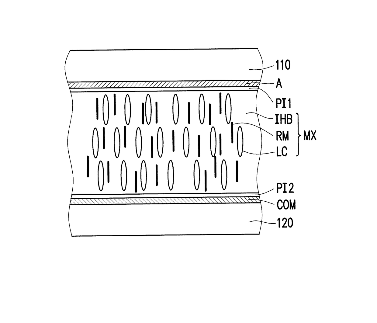
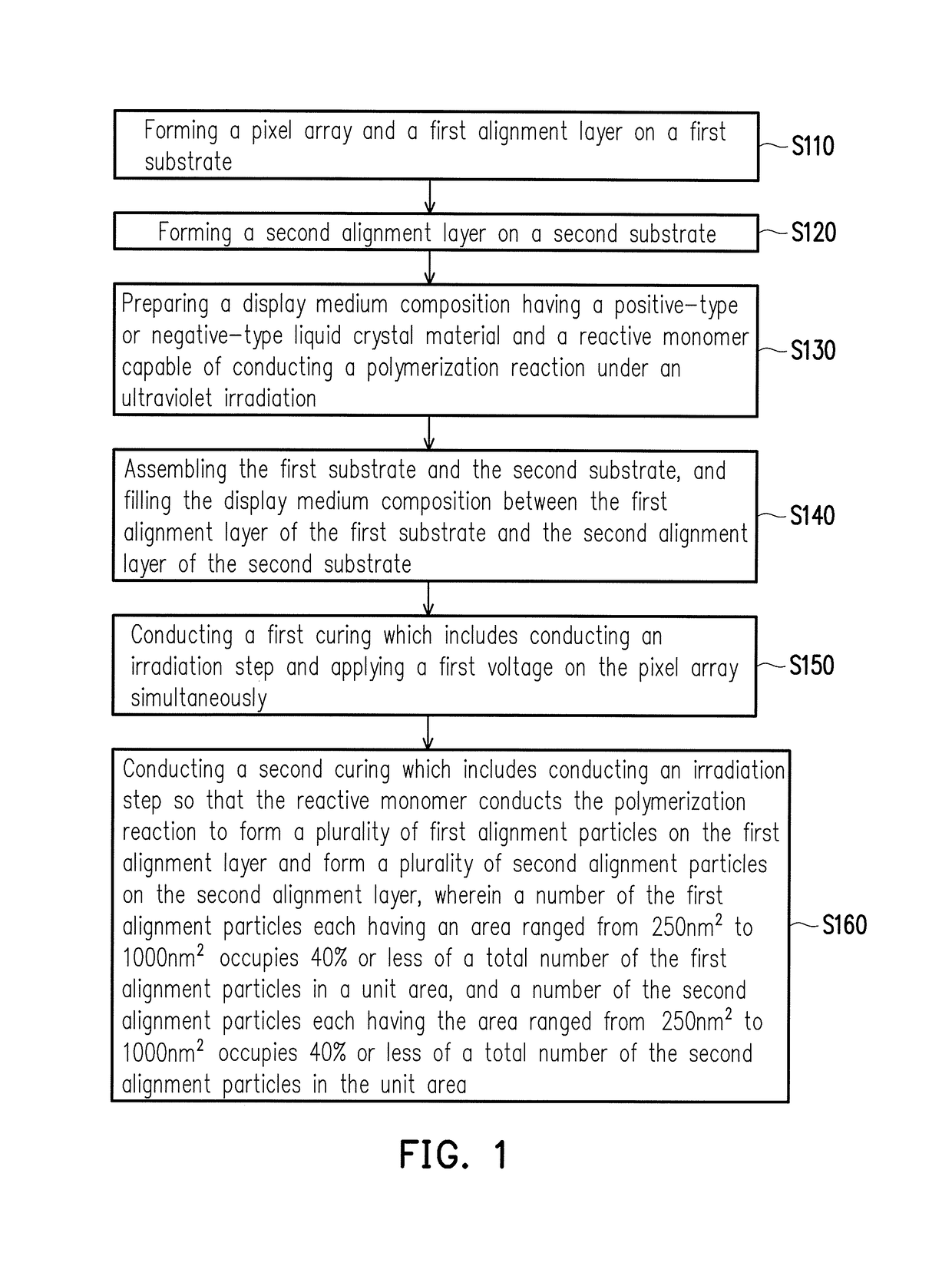
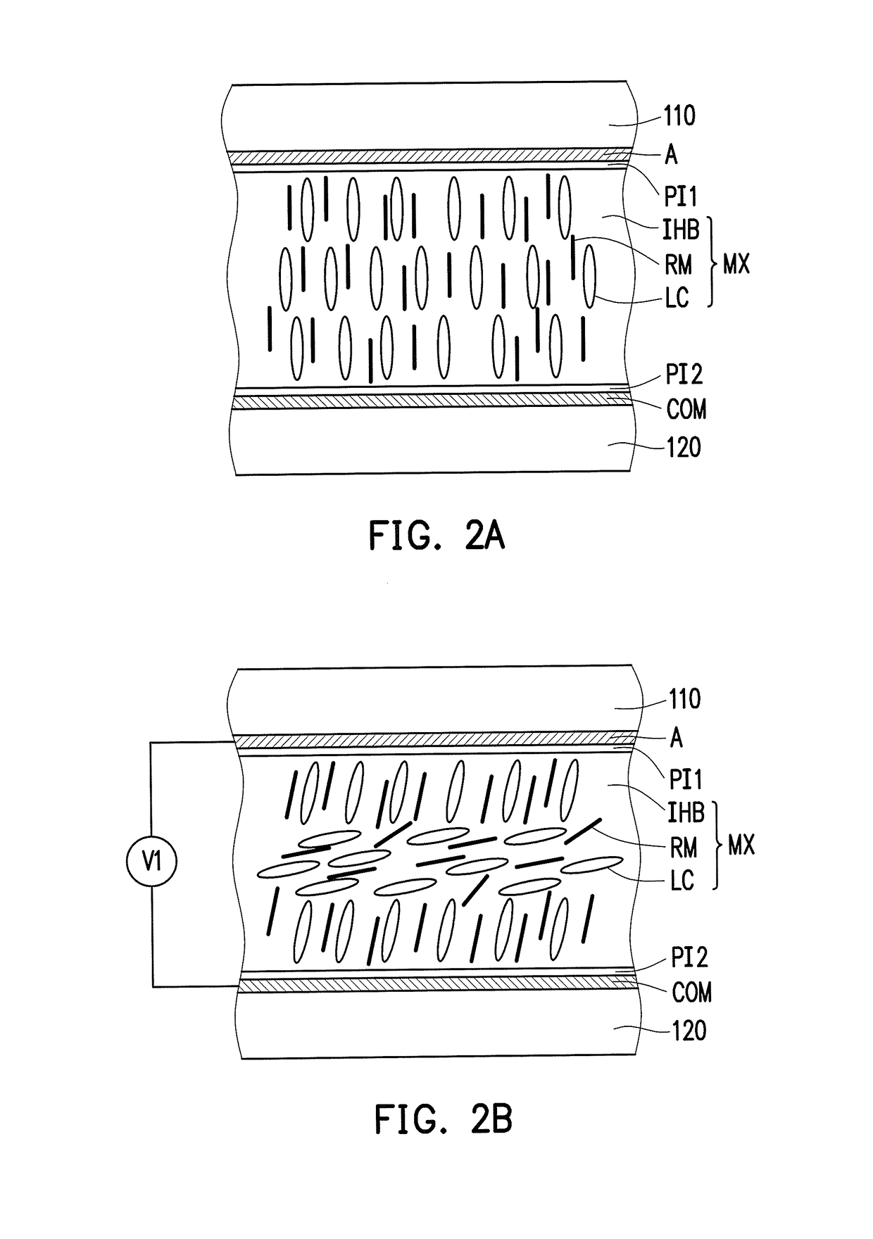
[0019]FIG. 1 is a flowchart of a manufacturing method of display panel according to an embodiment of the invention. Referring to FIG. 1, the manufacturing method of display panel includes the following steps. A pixel array and a first alignment layer are formed on a first substrate (step S110); a second alignment layer is formed on a second substrate (step S120); a display medium composition including a positive-type or negative-type liquid crystal material and a reactive monomer capable of conducting a polymerization reaction under an ultraviolet irradiation is prepared (step S130); the first substrate and the second substrate are assembled together, and the display medium composition is filled betw...


PUM

PropertyMeasurementUnit
areaaaaaaaaaaa
areaaaaaaaaaaa
areaaaaaaaaaaa

Abstract

A display panel including a first substrate, a pixel array disposed on the first substrate, a first alignment layer covering the pixel array, a second substrate disposed opposite the first substrate, a second alignment layer disposed on the second substrate and a display medium disposed between the first alignment layer and the second alignment layer is provided. The first alignment layer has first alignment particles. A number of the first alignment particles each having an area ranged from 250 nm2 to 1000 nm2 occupies 40% or less of a total number of the first alignment particles in a unit area. The second alignment layer has second alignment particles. A number of the second alignment particles each having the area ranged from 250 nm2 to 1000 nm2 occupies 40% or less of a total number of the second particles in the unit area.

Description

CROSS-REFERENCE TO RELATED APPLICATION[0001]This application claims the priority benefit of Taiwan application serial no. 104122248, filed on Jul. 9, 2015. The entirety of the above-mentioned patent application is hereby incorporated by reference herein and made a part of this specification.BACKGROUND OF THE INVENTION[0002]Field of the Invention[0003]The invention relates to an electronic apparatus, and more particularly, to a display panel.[0004]Description of Related Art[0005]Conventionally, the multi-domain vertically aligned liquid crystal display (MVA) LCD panel utilizes an alignment structure to make liquid crystal molecules in different regions tilt at different angles in order to achieve the effect of wide viewing angle. The alignment structure includes alignment protrusions and alignment slits disposed on pixel electrodes. However, a contrast ratio of the LCD panel may be lowered because of a light leakage usually caused by the disclination of tilting directions of the liqu...

Claims


Application Information

Patent Timeline
Patent Type & Authority Patents(United States)
IPC IPC(8): C09K19/00G02F1/1337G02F1/1341
CPCG02F1/1337G02F1/1341G02F1/133788Y10T428/10Y10T428/1005G02F1/133711G02F1/133715C09K2323/02C09K2323/00G02F1/133776
Inventor LIN, CHEN-CHUNTING, TIEN-LUNHSU, WEN-HAO
Owner AU OPTRONICS CORP
Why Eureka
Try Eureka