Combined SADP fins for semiconductor devices and methods of making the same

a semiconductor device and self-aligning technology, applied in the field of semiconductor devices, can solve the problems of increasing difficulty in achieving variable pitch, or variable spacing between fins in the fin field effect transistor (finfet), and difficulty in achieving variable spacing with conventional saqp between fins within an array of five or more fins, so as to achieve more variable spacing

Active Publication Date: 2017-06-27
GLOBALFOUNDRIES US INC
View PDF26 Cites 18 Cited by
  • Summary
  • Abstract
  • Description
  • Claims
  • Application Information

AI Technical Summary

Benefits of technology

[0007]The present invention offers advantages and alternatives over the prior art by providing a semiconductor cell or similar structure and method of making the same. The fabrication of the semiconductor cell can achieve a more variable spacing between fins in an array using standard lithog...

Problems solved by technology

Moreover, variable pitch, or variable spacing between fins in a Fin Field Effect Transistor (FinFET), is very difficult to achieve with SAQP.
More specifically, achieving variable spacing with conventional SAQP between fins within an array of five fins or more is increasingly difficult when the sp...

Method used


Image

  • Combined SADP fins for semiconductor devices and methods of making the same
  • Combined SADP fins for semiconductor devices and methods of making the same
  • Combined SADP fins for semiconductor devices and methods of making the same

Examples


Embodiment Construction

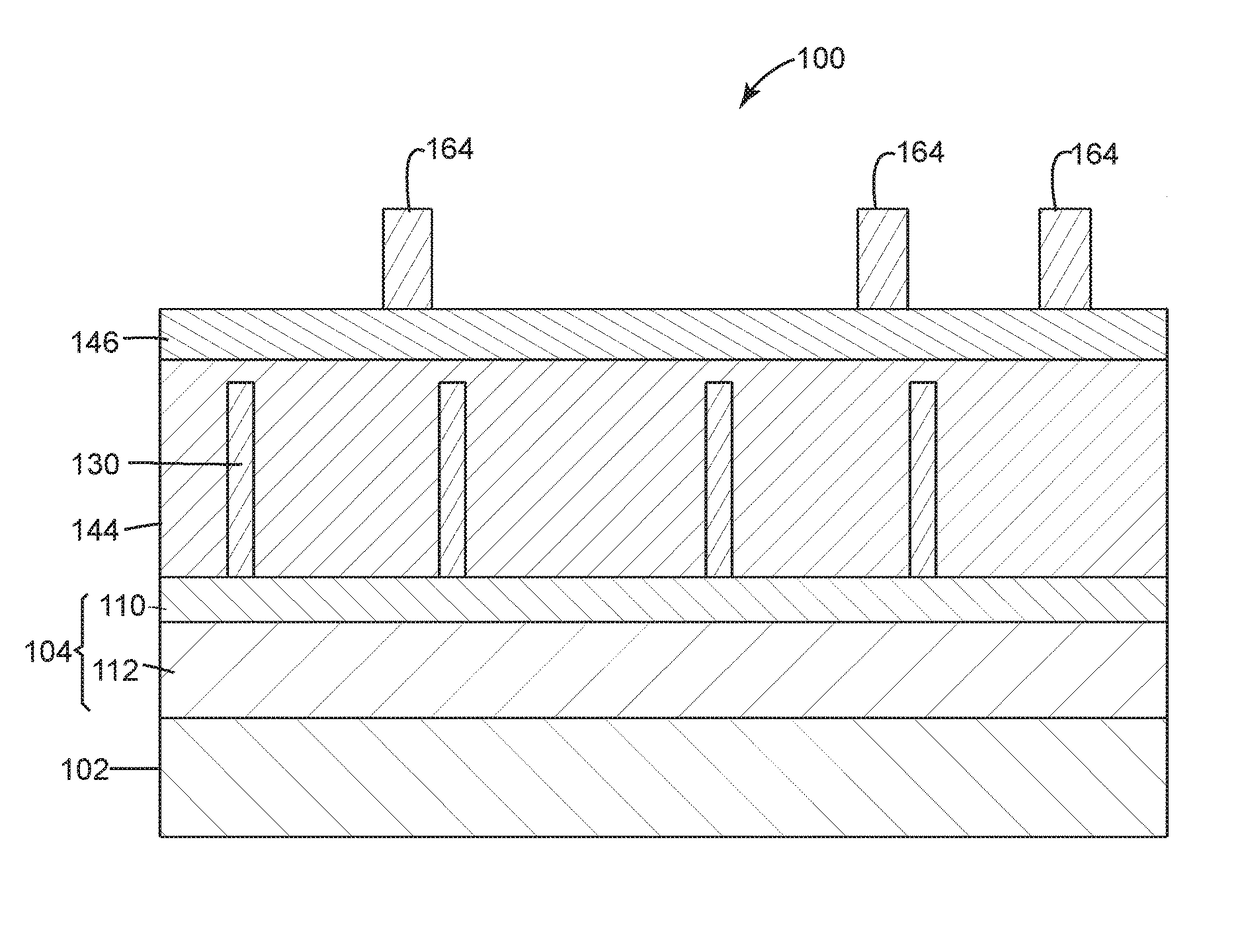
[0042]Certain exemplary embodiments will now be described to provide an overall understanding of the principles of the structure, function, manufacture, and use of the methods, systems, and devices disclosed herein. One or more examples of these embodiments are illustrated in the accompanying drawings. Those skilled in the art will understand that the methods, systems, and devices specifically described herein and illustrated in the accompanying drawings are non-limiting exemplary embodiments and that the scope of the present invention is defined solely by the claims. The features illustrated or described in connection with one exemplary embodiment may be combined with the features of other embodiments. Such modifications and variations are intended to be included within the scope of the present invention.

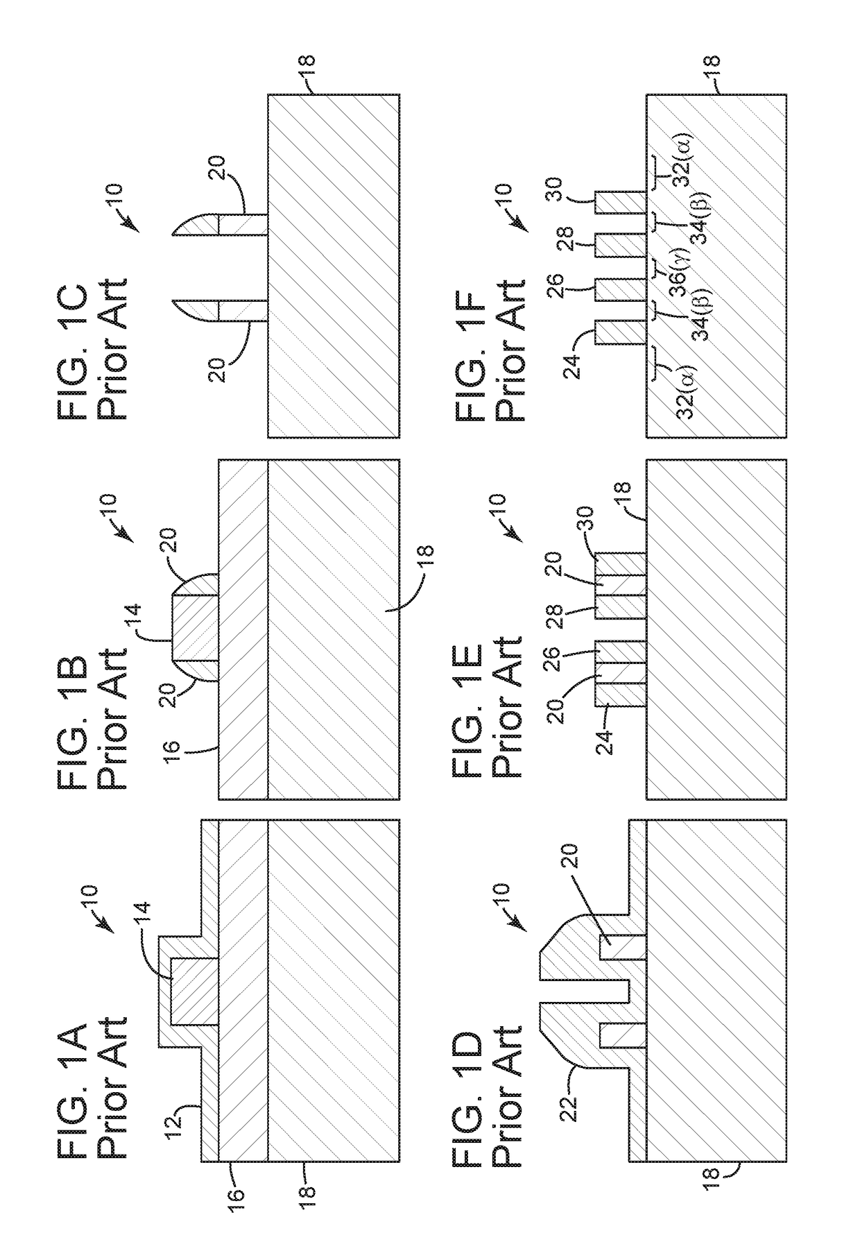
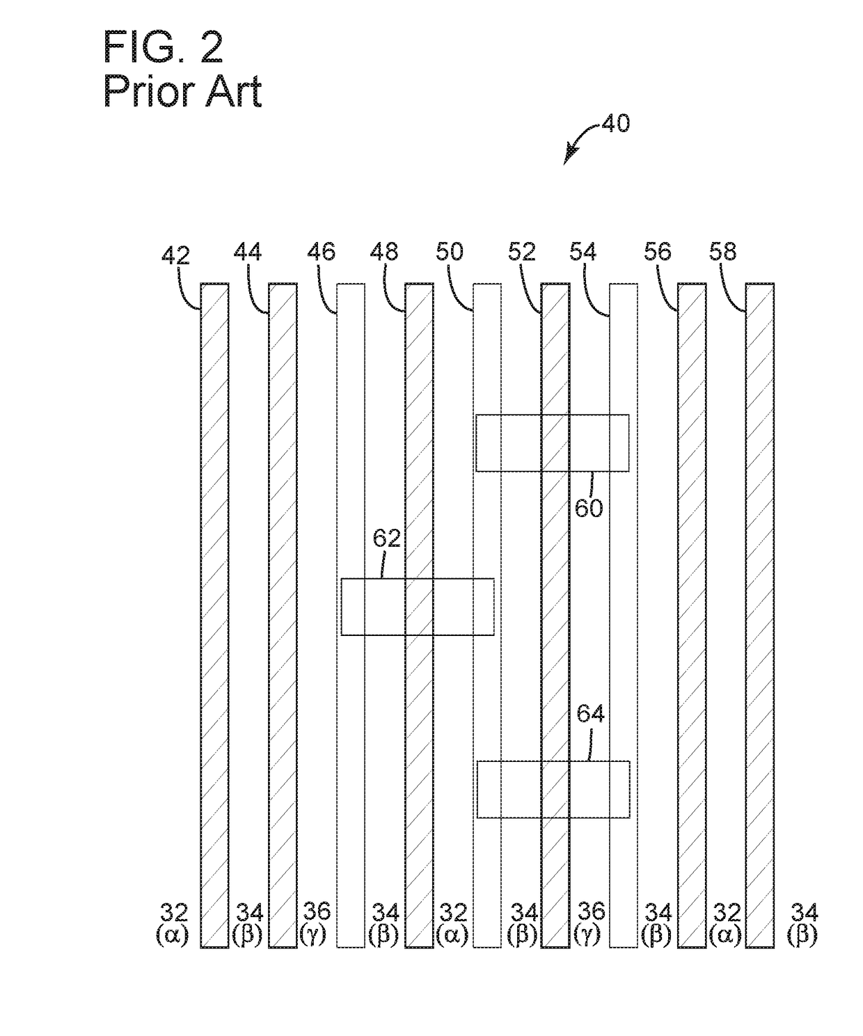
[0043]FIGS. 1A-1F illustrate a typical prior art SAQP method of semiconductor fabrication. FIG. 2 illustrates a typical prior art SRAM cell including n-type, p-type fins and dummy ...


PUM


Abstract

A semiconductor cell includes a substrate and an array of at least five substantially parallel fins having substantially equal fin widths disposed on the substrate. The array includes a predetermined minimum spacing distance between at least one pair of adjacent fins within the array. The array has a first n-type fin for an n-type semiconductor device, and a first p-type fin for a p-type semiconductor device. The first p-type fin is disposed adjacent the first n-type fin and spaced a predetermined first n-to-p distance apart from the first n-type fin. The first n-to-p distance is greater than the minimum spacing distance and less than the sum of the fin width plus twice the minimum spacing distance.

Description

TECHNICAL FIELD[0001]The present invention relates to semiconductor devices and methods of fabricating the same. More specifically, the invention relates to combined self-aligned double patterning fins for semiconductor devices and methods of making the same.BACKGROUND[0002]Technologies for fabricating semiconductor devices, such as transistors, capacitors and the like, for ultra-high density integrated circuits have been developed which extend patterning resolution beyond that of conventional lithography (which is typically limited to about 80 nm pitch). Self-aligned multiple patterning is one such class of high resolution patterning technologies. The current state of the art multiple patterning technology contemplated for commercial production is a method known as Self-Aligned Quadruple Patterning (SAQP), which is an extrapolation of the more commonly commercially used Self-Aligned Double Patterning (SADP) technique.[0003]Problematically, the theoretical minimum regular pitch for ...

Claims


Application Information

Patent Timeline
IPC IPC(8): H01L27/11H01L21/311H01L27/02H01L27/092H01L21/3105H01L21/308H01L21/8238
CPCH01L27/1104H01L27/0924H01L27/0207H01L21/823821H01L21/3081H01L21/31051H01L21/31111H01L21/823431H01L27/0886H10B10/12H01L21/3086
Inventor LICAUSI, NICHOLAS VINCENTKOZARSKY, ERIC SCOTTBOUCHE, GUILLAUME
Owner GLOBALFOUNDRIES US INC
Why Eureka
Try Eureka