Light emitting device package

a light-emitting device and light-emitting device technology, applied in the direction of semiconductor devices, basic electric elements, electrical equipment, etc., can solve the problems of affecting the production efficiency of vcsel and vecsel devices with some wavelengths, the light emitted by such devices may be considered cold, and the manufacturing method is convenient and the effect of high precision

Active Publication Date: 2017-06-27
LUMILEDS
View PDF5 Cites 1 Cited by
  • Summary
  • Abstract
  • Description
  • Claims
  • Application Information

AI Technical Summary

Benefits of technology

[0020]In the case of this packaged device, solder covers the at least one bonding area completely but not the surrounding area(s). This makes the assembly of the die into the package body more straightforward, since the reflective material surrounding the at least one solder bonding area may act as a solder relief or solder resist giving rise to self-alignment of the solder because wetting of regions with solder apart from the solder bonding area is prevented or reduced.
[0040]Alternatively, the provision of metal coating layers on the leadframe may be avoided. The avoidance of a silver coating can enhance adhesion. Thus, the leadframe may be of copper or copper alloy without any additional layers when the leadframe is introduced into the mould.

Problems solved by technology

LED technology does not represent the only way to generate light in solid state devices.
The reason for using phosphors with such devices is that there are technical difficulties in producing VCSEL and VECSEL devices with some wavelengths.
However, the light emitted by such devices may be considered cold and it would therefore be beneficial to provide a warmer light color.
This may be prone to degradation in the form of tarnishing which can color the reflective metal layer and lead to reduced reflectivity.
A further issue is the weak adhesion of mould compound to Ag leading to delamination risks.

Method used


Image

  • Light emitting device package
  • Light emitting device package
  • Light emitting device package

Examples


Embodiment Construction

[0054]The invention provides a method of packaging a light emitting device and a packaged light emitting device.

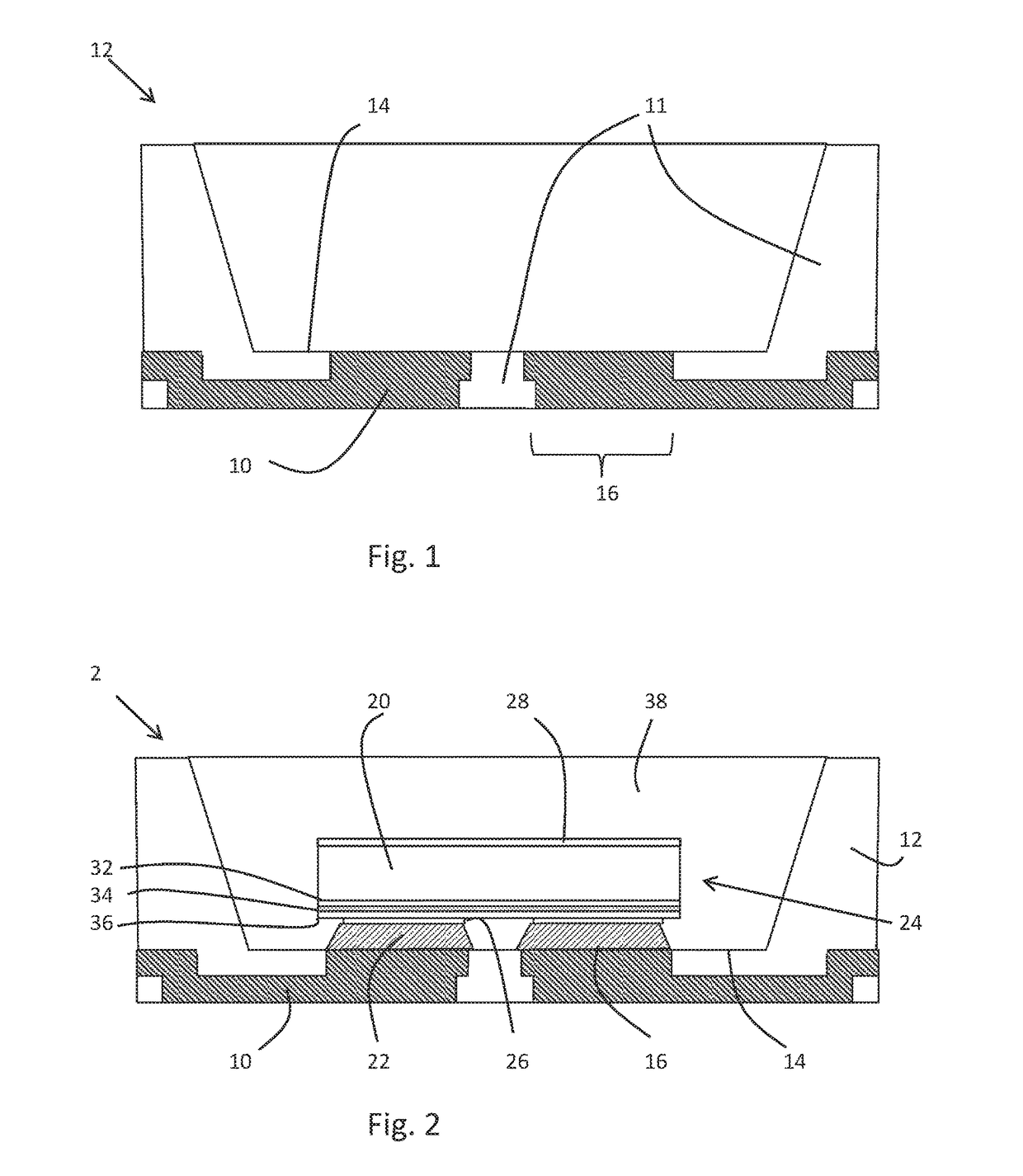
[0055]Referring to FIG. 1, a general view of a package is shown. FIG. 2 shows a packaged light emitting device, i.e. a light emitting device die in the package of FIG. 1. In this example the light emitting device is a LED but similar packaging approaches may be used for other solid state light emitting devices.

[0056]Referring to FIG. 1, a profiled leadframe 10 is made of Cu and has been etched to have a particular profile or shape, for example the leadframe 10 has a varying thickness as illustrated in FIG. 1, and / or the leadframe 10 has a shape with dimensions that vary at least in two directions. The thickness is in this case defined as the distance between an upper surface of the leadframe 10, on which the bonding will be done, and a surface opposite to this bonding surface. As can be seen in FIG. 1 leadframe 10 has a profile or shape in which an upper surface of the lea...


PUM

PropertyMeasurementUnit
thicknessaaaaaaaaaa
thicknessaaaaaaaaaa
areaaaaaaaaaaa

Abstract

A packaged light emitting device die includes a package body having a profiled leadframe embedded in a body of reflecting material. The leadframe is exposed on mounting surface only on at least one solder bonding area. Solder is present only on the at least one solder bonding area and not elsewhere. The reflecting material provides the reflecting parts of the package so there is no need for a reflective layer to be deposited on leadframe. Moreover, the reflecting material can function as a solder resist to self-align the solder to the at least one solder bonding area.

Description

CROSS-REFERENCE TO RELATED APPLICATIONS[0001]The present application is a §371 application of International Application No. PCT / IB2015 / 050121 filed on Jan. 7, 2015 and entitled “LIGHT EMITTING DEVICE PACKAGE,” which claims priority to International Application No. PCT / CN2013 / 001603 filed on Dec. 19, 2013 and European Patent Application No. 14150307.8 filed on Jan. 7, 2014. International Application No. PCT / IB2015 / 050121, International Application No. PCT / CN2013 / 001603, and European Patent Application No. 14150307.8 are incorporated herein.FIELD OF THE INVENTION[0002]The invention relates to a packaged light emitting device, a package for a light emitting device and a method of manufacturing the packaged device.BACKGROUND OF THE INVENTION[0003]A number of different approaches to generate light from a solid state light emitting device are known.[0004]A very common approach is to use light emitting diodes (LEDs), which are in increasing use for a number of applications in view of their...

Claims


Application Information

Patent Timeline
Patent Type & Authority Patents(United States)
IPC IPC(8): H01L33/00H01L33/62H01L33/60H01L33/48
CPCH01L33/62H01L33/486H01L33/60H01L2224/16245H01L2224/32245H01L2224/48091H01L2224/48247H01L2224/73265H01L2933/0033H01L2933/0058H01L2933/0066H01L2924/00014H01L2924/00
Inventor DIJKSTRA, PAULREINTS BOK, AERNOUTOBERNDORFF, PASCAL JOHANNES THEODORUS LAMBERTUSZHANG, LU FEIDE JONG, BOUDEWIJN RUBENDONKER, MARCUS FRANCISCUS
Owner LUMILEDS
Why Eureka
Try Eureka