Display device and driving method thereof
a display device and driving method technology, applied in static indicating devices, instruments, electroluminescent light sources, etc., can solve the problem of inability to obtain clear display images, and achieve the effect of improving display quality and low power consumption
- Summary
- Abstract
- Description
- Claims
- Application Information
AI Technical Summary
Benefits of technology
Problems solved by technology
Method used
Image
Examples
embodiment 1
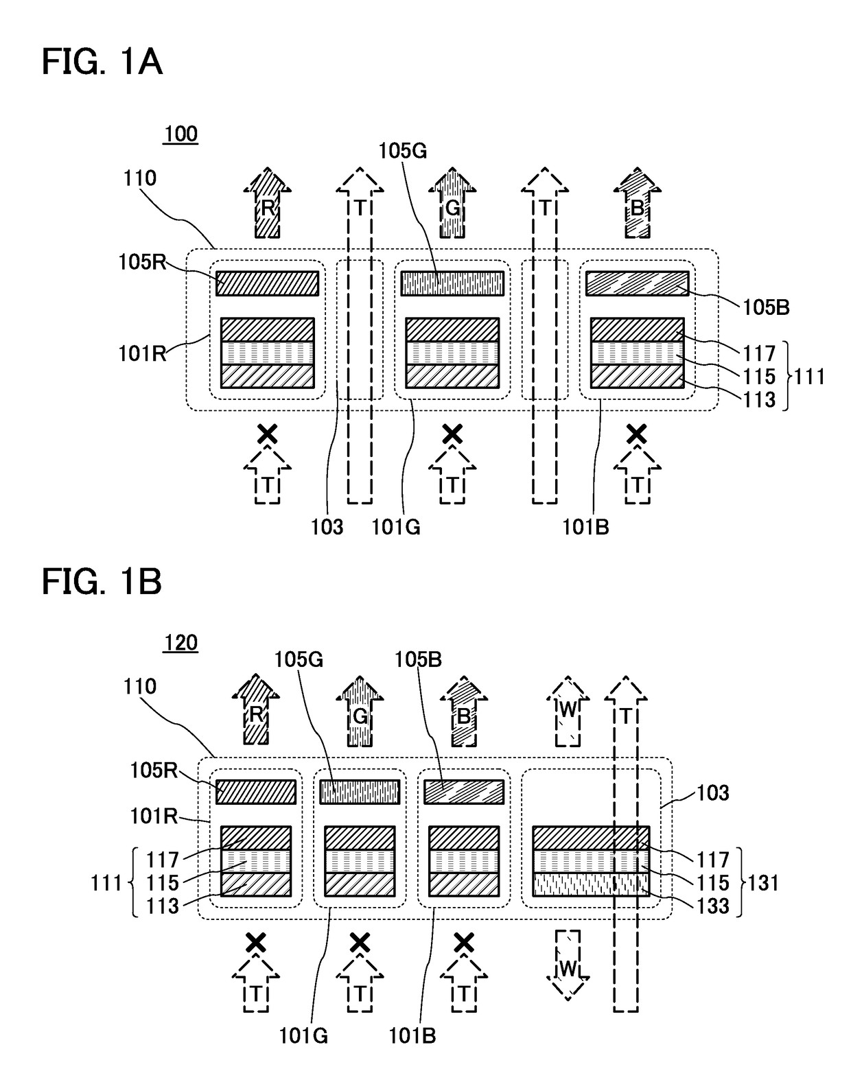
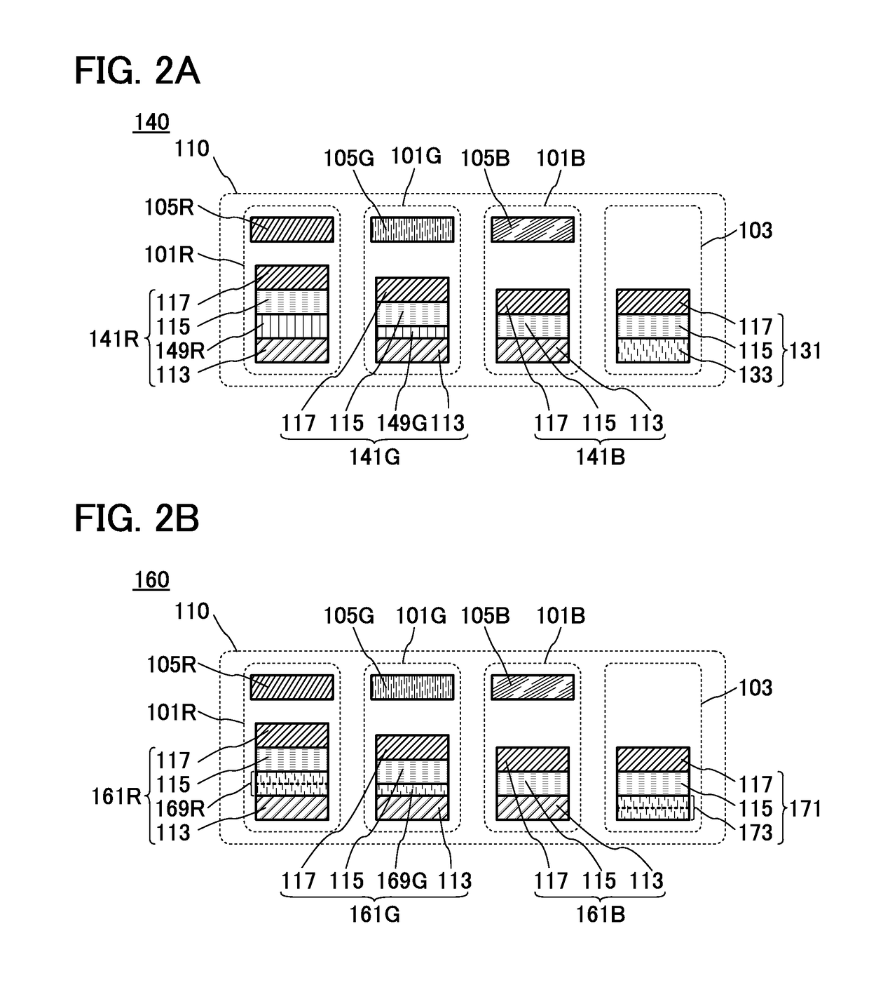
[0044]A structure example of a display device according to one embodiment of the present invention will be described with reference to FIGS. 1A and 1B, FIGS. 2A and 2B, FIGS. 3A to 3C, and FIGS. 4A to 4C.
[0045]FIG. 1A is a schematic diagram of a display device 100.
[0046]The display device 100 includes a plurality of pixels 110, and each pixel 110 includes a display element 101R emitting red light, a display element 101G emitting green light, a display element 101B emitting blue light, and a transmissive portion 103. Here, in the case where characteristics common to the display elements are described, these display elements are collectively referred to as a display element 101.
[0047]The display element 101R includes a light-emitting element 111 and a color filter 105R. Similarly, the display element 101G includes a light-emitting element 111 and a color filter 105G, and the display element 101B includes a light-emitting element 111 and a color filter 105B.
[0048]Here, in the display d...
embodiment 2
[0104]In this embodiment, a structure example of a display device including a transmissive light-emitting element in a transmissive portion will be described with reference to drawings.
[0105]The transmissive display device according to one embodiment of the present invention can employ either a simple matrix mode or an active matrix mode. An example of display device employing an active matrix mode will be described below.
[0106]FIG. 5A is a schematic top view of a display device 200 according to one embodiment of the present invention.
[0107]The display device 200 includes a first substrate 211 and a second substrate 212 which face each other. Over the first substrate 211, a display portion 201 including a plurality of pixels 110, a scan line driver circuit 202, and a signal line driver circuit 203 are provided. The first substrate 211 and the second substrate 212 are attached to each other with a sealant 213 surrounding the display portion 201, and a sealed region surrounded by the ...
structure example 3
[0127]The above structure examples shows a structure in which each of the display elements and the transmissive portion have almost the same area; however, it is preferable to increase the area of the transmissive portion by having different structures of the light-emitting element and the transmissive light-emitting element. A structure example where the area of the transmissive portion is made larger than that of each display element will be described below.
[0128]FIG. 6B is a schematic top view of a region including a pixel 110. The pixel 110 which will be described in this structure example as an example is different from that in Structure Example 1 in the area occupied by one pixel 110 and the shape of the transmissive portion 103.
[0129]Here, the pixel 110 is divided into two rows: three display elements (the display elements 101R, 101G, and 101B) are arranged in one row, and the other row is occupied by one transmissive portion 103.
[0130]The third electrode layer 133 in the tra...
PUM
 Abstract
Description
Claims
Application Information


