Solar cell module

a solar cell and module technology, applied in the field of solar cell modules, can solve the problems of low collection efficiency of photogenerated carriers (electron or positive holes), and achieve the effect of preventing degradation of photogenerated carrier collection efficiency

Active Publication Date: 2017-08-08
PANASONIC INTELLECTUAL PROPERTY MANAGEMENT CO LTD
View PDF7 Cites 0 Cited by
  • Summary
  • Abstract
  • Description
  • Claims
  • Application Information

AI Technical Summary

Benefits of technology

[0009]In the abovementioned solar cell module, each n-type side electrode in the first solar cell and wiring member are electrically separated and each p-type side electrode within the second solar cell and wiring member are electrically separated. Hence, each p-type side electrode in the first solar cell and each n-type side electrode in the second solar cell can be connected electrically by wiring member. Therefore, it is not necessary to place a connecting electrode in order to connect to wiring member in each solar cell. Thus, it can prevent degradation of collection efficiency of photogenerated carriers.

Problems solved by technology

However, in the region of the back side of semiconductor substrate, wherein n-type side connecting electrode and p-type side connecting electrode are arranged, low collection efficiency of photogenerated carriers (electron or positive hole) has been a problem.

Method used


Image

  • Solar cell module
  • Solar cell module
  • Solar cell module

Examples


second embodiment

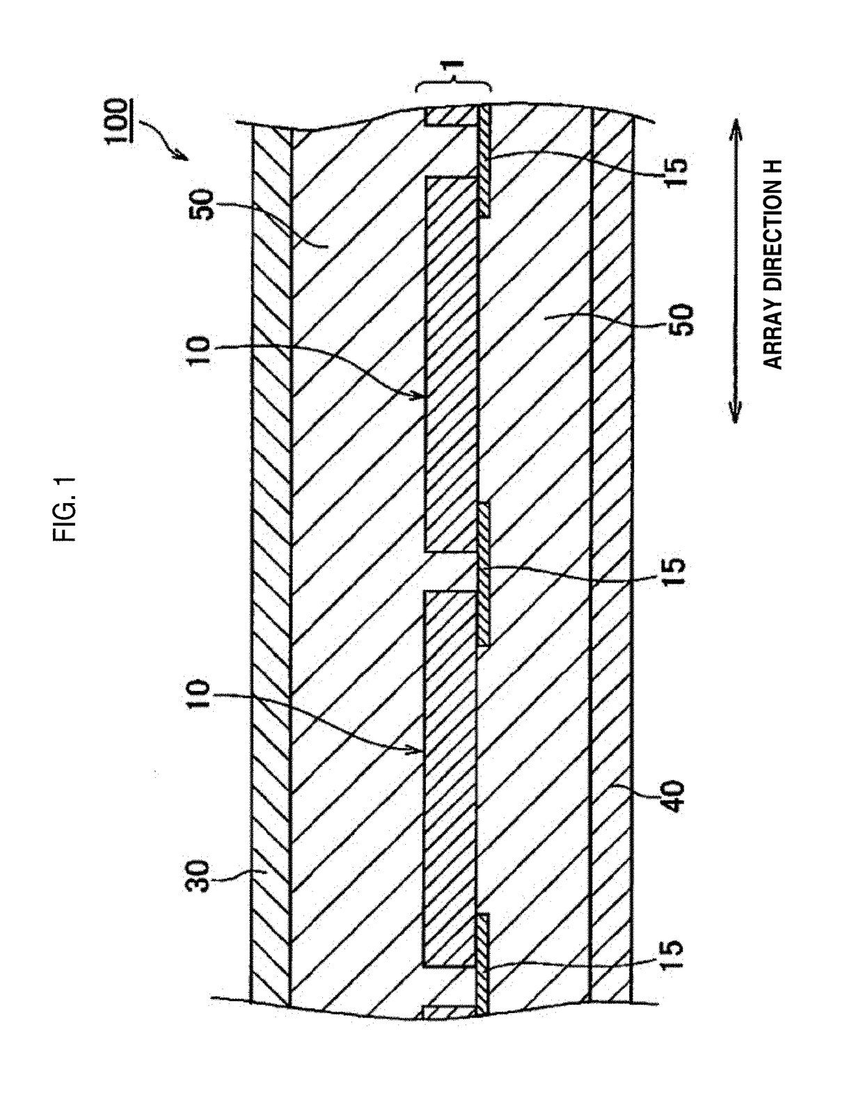
[0056]Next, with reference to the drawings, a second embodiment is described. A solar cell module in this embodiment has a similar configuration as above-described solar cell module 100 in the first embodiment. (referred to FIG. 1 and FIG. 2) In the following description, differences between the second embodiment and above-described first embodiment are chiefly described.

(Configuration of a Solar Cell)

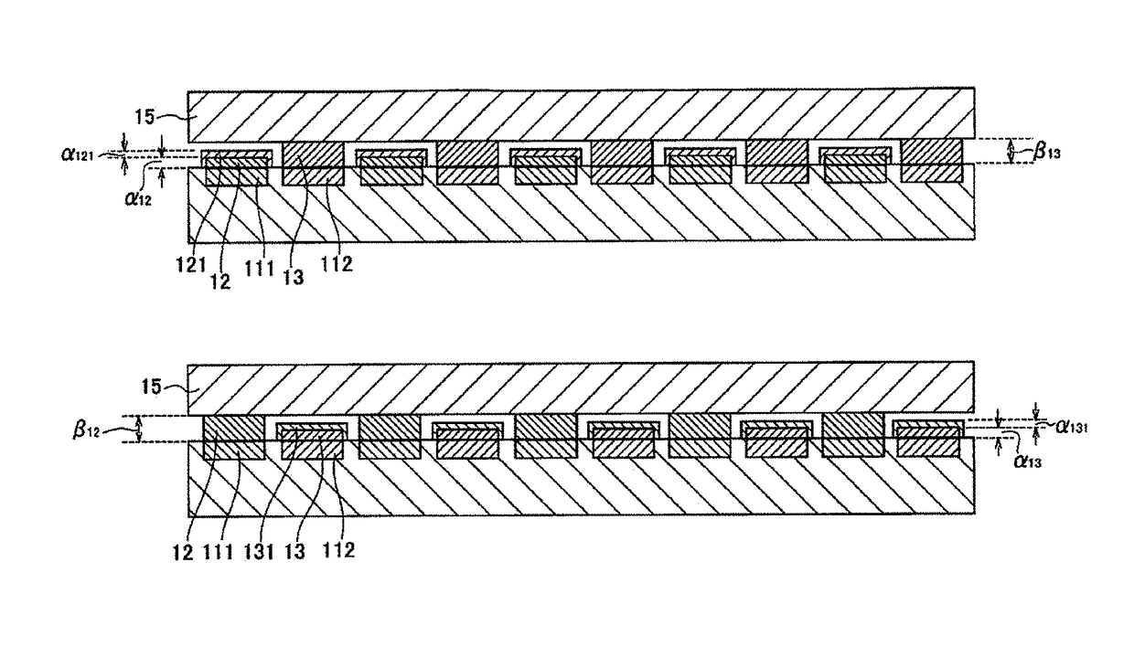
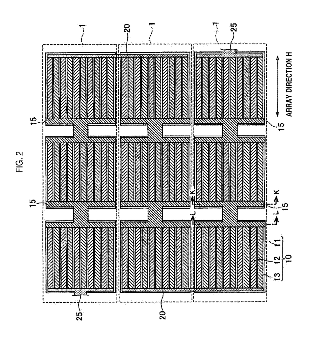
[0057]FIG. 8A is a cross-sectional view taken along sectional line L-L of FIG. 2. FIG. 8B is a cross-sectional view taken along sectional line K-K of FIG. 2.

[0058]As shown in FIG. 8A, illustrating one solar cell 10, α12 indicates the thickness of the part of each n-type side electrode 12, which is facing wiring member 15. β13 indicates the thickness of the part of each p-type side electrode 13, which is facing wiring member 15. Thickness α12 is thinner than the thickness β13. Furthermore, thickness β13 is greater than total thickness of α121 and thickness α12 of n-type side cover 121. ...

working example 1

[0079]Firstly, n-type single-crystalline silicon substrate is prepared. It is formed approximately 100 mm square and thickness 200 μm and its resistivity is 0.1 Ωcm.

[0080]Next, by using screen printing method, n-type diffusing agent paste (containing phosphorus) and p-type diffusing agent paste (containing boron) are printed in lines, each agent forming 41 lines on the back surface of n-type single-crystalline silicon substrate, respectively. Further, by applying thermal diffusion treatment, 41 lines of each of n-type region and p-type region having 0.8 mm in width and 98 mm in length are formed at intervals of 2.4 mm.

[0081]Next, transparent conducting layer (ITO layer) is formed on respective n-doped region and p-doped region by sputtering method. After silver paste is printed on ITO layer by using screen printing method, n-type side electrode and p-type side electrode are formed. The dimension of each electrode is 0.8 mm in width, 98 mm in length and 30 μm in thickness. Then n-typ...

working example 2

[0086]In working example 2, thickness of silver paste, which is formed on n-type side cover above n-type side electrode, is formed 10 μm thinner than other surface area. Due to the fact that the thickness of n-type side cover is 10 μm; the surface of n-type side electrode and the surface of n-type side cover are even in thickness.

[0087]Similarly, thickness of silver paste, which is formed on p-type side cover above p-type side electrode, is formed 10 μm thinner than other surface area. Due to the fact that the thickness of p-type side cover is 10 μm; the surface of p-type side electrode and the surface of p-type side cover are even in thickness.

[0088]All other processes in working example 2 are the as above-described working example 1.


PUM


Abstract

A first solar cell is electrically connected to a second solar cell electrically and arranged in an array direction. Each of the first and second solar cell comprises: a light-receiving surface; a rear surface; a plurality of n-type side electrodes and p-type side electrodes both formed in the array direction on the rear surface; a wiring member electrically connecting the first solar cell and the second solar cell and arranged over the plurality of n-type side electrodes and the plurality of p-type side electrodes; an n-type side electrode insulating member that is arranged over the wiring member and covers a part of the plurality of n-type side electrodes, the part facing the wiring member; and a p-type side electrode insulating member that is arranged over the wiring member and covers a part of the plurality of p-type side electrodes, the part facing the wiring member.

Description

CROSS REFERENCE TO RELATED APPLICATIONS[0001]This application claims priority based on 35USC119 from prior Japanese Patent Application No. P2008-205878 filed on Aug. 8, 2008, entitled “SOLAR CELL MODULE”, the entire contents of which are incorporated herein by reference.BACKGROUND OF THE INVENTION[0002]1. Field of the Invention[0003]The invention relates to a solar cell module including back junction solar cell.[0004]2. Description of Related Art[0005]A solar cell is considered as a new prospective source of energy because it can convert clean and inexhaustible supply of sunlight directly into electricity. Each solar cell can often produce only about a few watts of power. Hence, a solar cell module is used when solar cells are utilized to supply electrical power (energy source) to residential homes or buildings. A solar cell module is created by connecting individual solar cells electrically in order to increase electrical power output.[0006]Here, Japanese Patent Laid-Open No. 2005-...

Claims


Application Information

Patent Timeline
Patent Type & Authority Patents(United States)
IPC IPC(8): H01L31/00H01L31/0224H01L31/05
CPCH01L31/022433H01L31/0516Y02E10/50
Inventor MISHIMA, TAKAHIROSAKATA, HITOSHI
Owner PANASONIC INTELLECTUAL PROPERTY MANAGEMENT CO LTD
Why Eureka
Try Eureka