Transparent photovoltaic cells

a photovoltaic cell and transparent technology, applied in the field of photovoltaic devices, can solve the problems of limited mechanical flexibility, high module cost, and the surface area necessary to take advantage of solar energy remains an obstacle to offset a significant portion of non-renewable energy consumption, and achieve the effect of maximizing the absorption of near infrared light in the infrared-absorbing active layer

Active Publication Date: 2017-08-08
MASSACHUSETTS INST OF TECH
View PDF27 Cites 13 Cited by
  • Summary
  • Abstract
  • Description
  • Claims
  • Application Information

AI Technical Summary

Benefits of technology

[0009]A method of fabricating a photovoltaic cell may include fabricating a first electrode material on a substrate, the electrode material and the substrate being transparent to visible light. At least one layer may be fabricated, the layer having a first active material with an absorption peak at a wavelength greater than about 650 nanometers and a second active material with an absorption peak at a wavelength outside of the visible light spectrum. A second electrode may be fabricated of material transparent to visible light. The method may include selecting a thickness of at least one of the first or second electrodes such that absorption of near infrared light in the infrared-absorbing active layer is maximized. The method may also include fabricating a multi-layer mirror for near-infrared light.

Problems solved by technology

The surface area necessary to take advantage of solar energy remains an obstacle to offsetting a significant portion of non-renewable energy consumption.
The limited mechanical flexibility, high module cost and, more importantly, the band-like absorption of inorganic semiconductors limit their potential utility to transparent solar cells.
Previous efforts to construct semitransparent devices have focused on the use of thin active layers (or physical holes) with absorption focused in the visible spectrum and therefore have been limited to either low efficiencies <1% or low average visible transmissivity (AVT) to light around 10-35%, since both parameters cannot be simultaneously optimized.

Method used


Image

  • Transparent photovoltaic cells
  • Transparent photovoltaic cells
  • Transparent photovoltaic cells

Examples


Embodiment Construction

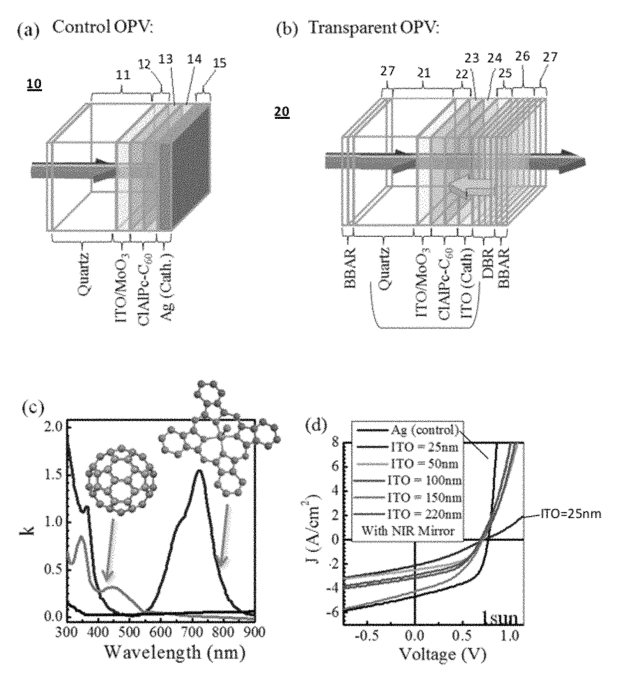
[0037]Described herein are improved transparent solar cell designs, e.g., transparent organic photovoltaic devices (TOPV). The term transparent as used herein encompasses an average visible transparency of a straight through beam of 45% or more. The term semi-transparent as used herein encompasses an average visible transparency of a straight through beam of approximately 10%-45%. In general, the designs include molecular active layers with strong absorption features outside of the visible light spectrum, e.g., in the ultra-violet (UV) and / or near-infrared (NIR) solar spectrum. The devices may include selective high-reflectivity NIR and broadband anti-reflection contact coatings. Devices may be formed as heterojunction solar cells with an organic active layer, such as chloroaluminum phthalocyanine (ClAlPc) or SnPc as a donor and a molecular active layer such as C60 acting as an acceptor and having peak-absorption in the UV and NIR solar spectrum. Other suitable materials for the act...


PUM


Abstract

A transparent photovoltaic cell and method of making are disclosed. The photovoltaic cell may include a transparent substrate and a first active material overlying the substrate. The first active material may have a first absorption peak at a wavelength greater than about 650 nanometers. A second active material is disposed overlying the substrate, the second active material having a second absorption peak at a wavelength outside of the visible light spectrum. The photovoltaic cell may also include a transparent cathode and a transparent anode.

Description

CROSS-REFERENCE TO PRIOR FILED APPLICATION[0001]This application claims priority to earlier filed provisional application 61 / 436,671 filed on Jan. 26, 2011, which is herein incorporated by reference in its entirety.FIELD OF INVENTION[0002]This invention relates to the field of photovoltaic devices and more particularly, organic photovoltaic devices.BACKGROUND[0003]The surface area necessary to take advantage of solar energy remains an obstacle to offsetting a significant portion of non-renewable energy consumption. For this reason, low-cost, transparent, organic photovoltaic (OPV) devices that can be integrated onto window panes in homes, skyscrapers, and automobiles are desirable. For example, window glass utilized in automobiles and architecture are typically 70-80% and 55-90% transmissive, respectively, to the visible spectrum, e.g., light with wavelengths from about 450 to 650 nanometers (nm). The limited mechanical flexibility, high module cost and, more importantly, the band-l...

Claims


Application Information

Patent Timeline
Patent Type & Authority Patents(United States)
IPC IPC(8): H01L51/42H01L27/30H01L51/44
CPCH01L51/4213H01L27/302H01L51/4246H01L51/4253H01L51/442H01L51/447Y02E10/549H10K30/57H10K30/10H10K30/211H10K30/87H10K30/82H10K30/30H10K2102/351
Inventor BULOVIC, VLADIMIRLUNT, RICHARD ROYAL
Owner MASSACHUSETTS INST OF TECH
Why Eureka
Try Eureka