Variable capacitance device and antenna device

a capacitance device and variable technology, applied in the incorporation of printed capacitors, printed circuits, electrical devices, etc., can solve the problems of changing the capacitance of ceramic capacitors, current leakage problems in such devices, and mechanical reliability issues

Inactive Publication Date: 2017-08-08
TAIYO YUDEN KK
View PDF8 Cites 2 Cited by
  • Summary
  • Abstract
  • Description
  • Claims
  • Application Information

AI Technical Summary

Benefits of technology

[0013]An object of the present invention is to provide a relatively simple and effective way and structure to prevent current leakage in and increase the mechanical reliability of a variable capacitance device.
[0015]To achieve these and other advantages and in accordance with the purpose of the present invention, as embodied and broadly described, in one aspect, the present disclosure provides a variable capacitance device, including: a supporting substrate having a plurality of variable capacitance elements formed thereon, the plurality of variable capacitance elements being connected in series, wherein each of the plurality of variable capacitance elements includes: a lower electrode formed over the supporting substrate; a dielectric formed on the lower electrode; and an upper electrode formed on the dielectric, wherein each of the plurality of variable capacitance elements has a separate lower electrode, or at least some of the plurality of variable capacitance elements share a lower electrode, thereby forming a plural set of the lower electrodes that serves as the lower electrodes of the respective variable capacitance elements, wherein the variable capacitance device further includes an insulating moisture-resistant film and a conductive adhesive film that are formed after the upper electrodes for the respective variable capacitance elements have been formed, whereby the insulating moisture-resistant film and the conductive adhesive film are in layers that are positioned at a level higher than a layer in which the upper electrodes are formed, and wherein the conductive adhesive film and the insulating moisture-resistant film have a gap in a plan view between at least some of regions where the plural set of the lower electrodes are respectively formed so as to avoid electrical leakage between said at least some of regions through the conductive adhesive film.
[0016]Using a variable capacitance device with such a configuration prevents current leakage from occurring between lower electrode regions.

Problems solved by technology

The capacitance of ceramic capacitors changes over time when bias voltage is applied, however, which is a problem.
There have been mechanical reliability issues and current leakage problems in such devices, however, depending on certain factors.

Method used


Image

  • Variable capacitance device and antenna device
  • Variable capacitance device and antenna device
  • Variable capacitance device and antenna device

Examples


Embodiment Construction

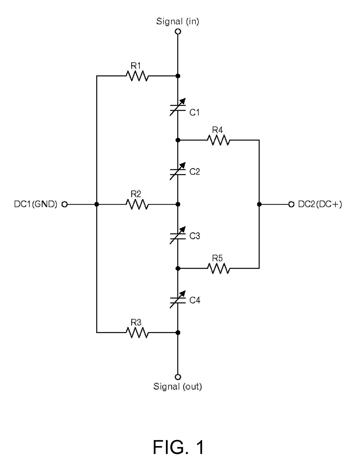
[0029]FIG. 1 shows an example of a circuit formed in a variable capacitance device according to an embodiment of the present invention. In the variable capacitance device shown in FIG. 1, a variable capacitance array containing variable capacitance elements C1 to C4 is connected in series from a high frequency signal input terminal (Signal(in)) to a high frequency signal output terminal (Signal(out)). In addition, for each of the variable capacitance elements C1 to C4 in the variable capacitance array, one end is connected to a ground terminal DC1 via resistors R1 to R3, and the other end is connected to a control voltage application terminal DC2 via resistors R4 and R5. The capacitance of the variable capacitance elements C1 to C4 in the variable capacitance array changes in accordance with voltage applied between the terminals DC2 and DC1.

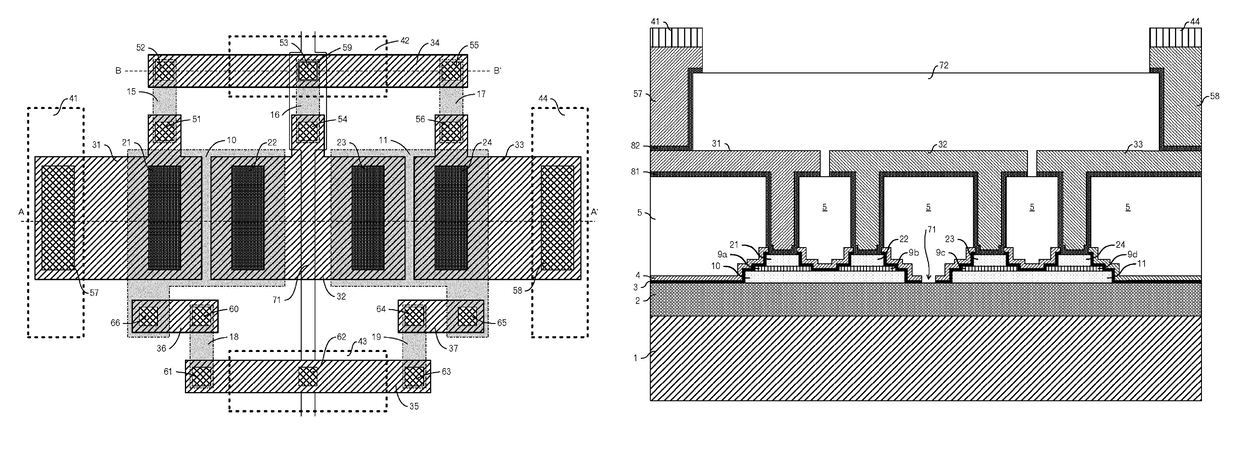
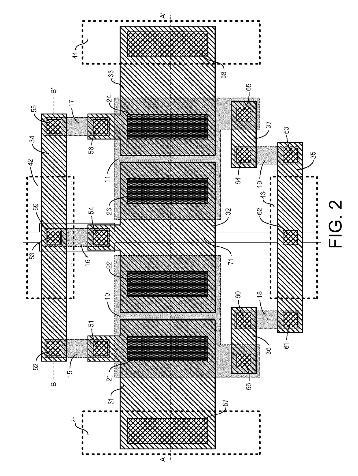
[0030]FIG. 2 is a transparent top view showing a basic configuration of the variable capacitance device of FIG. 1 in the case that the device is...


PUM


Abstract

A variable capacitance device includes: a supporting substrate having a plurality of variable capacitance elements formed thereon, the plurality of variable capacitance elements being connected in series, wherein each of the plurality of variable capacitance elements has a separate lower electrode, or at least some of the plurality of variable capacitance elements share a lower electrode, thereby forming a plural set of the lower electrodes that serves as the lower electrodes of the respective variable capacitance elements, wherein the variable capacitance device further includes an insulating moisture-resistant film and a conductive adhesive film, and wherein the conductive adhesive film and the insulating moisture-resistant film have a gap in a plan view between at least some of regions where the plural set of the lower electrodes are respectively formed so as to avoid electrical leakage between said at least some of regions through the conductive adhesive film.

Description

BACKGROUND OF THE INVENTION[0001]Technical Field[0002]The present invention relates to a variable capacitance device and an antenna device that utilizes the variable capacitance device.[0003]Background Art[0004]In NFC (near field communication) modules used for mobile FeliCa, a phenomenon has been known to occur in which reception sensitivity decreases as a result of the resonant frequency shifting away from 13.56 MHz due to variations in the antenna coil, for example. To correct these shifts in the resonant frequency, frequency adjustment circuits that include capacitors are placed inside the modules, all parts are inspected before the modules are shipped, and the capacitance of the capacitors is minutely adjusted.[0005]Conventionally, switched capacitors, in which FET (field effect transistor) switches are connected in series in a fixed capacitance element, have been used. Switchover settings are then written onto a control IC (integrated circuit) during the pre-shipping inspectio...

Claims


Application Information

Patent Timeline
Patent Type & Authority Patents(United States)
IPC IPC(8): H01G7/06H05K1/16
CPCH05K1/162H01G7/06H05K2201/10098
Inventor ISHII, DAIKIMORITO, KENTAROIKENAGA, TOMOKAZU
Owner TAIYO YUDEN KK
Why Eureka
Try Eureka