Check patentability & draft patents in minutes with Patsnap Eureka AI!

SRAM bitcell structures facilitating biasing of pass gate transistors

a technology of pass gate transistor and bitcell, which is applied in the field of static random access memory (sram) bitcell, can solve the problems of either failure of bitcell, read or write failure, etc., and achieve the effect of facilitating biasing

Active Publication Date: 2017-08-15
GLOBALFOUNDRIES US INC
View PDF1 Cites 6 Cited by
  • Summary
  • Abstract
  • Description
  • Claims
  • Application Information

AI Technical Summary

Benefits of technology

The present disclosure provides bitcell structures including semiconductor substrates with a deep n-well layer, p-well regions, and doped back-plate regions. The structures also include a buried oxide layer and a first polysilicon gate conductor overlapping a portion of the first active region. The structures further include at least one shallow trench isolation region and at least one contact to back plate region for biasing the transistors during read, write, or standby operations. The technical effect of the present disclosure is to provide more efficient and reliable bitcell structures with improved performance and reliability.

Problems solved by technology

A bitcell will fail either due to read or write failure.

Method used


Image

  • SRAM bitcell structures facilitating biasing of pass gate transistors
  • SRAM bitcell structures facilitating biasing of pass gate transistors
  • SRAM bitcell structures facilitating biasing of pass gate transistors

Examples


Embodiment Construction

,” one will understand how the features of the various embodiments disclosed herein provide a number of advantages over the current state of the art. These advantages may include, without limitation, providing 6T SRAM bitcells fabricated on a SOI substrate with improved Vmin and / or yield.

[0017]These and other features and advantages of this disclosure will become apparent from the following detailed description of the various aspects of the present disclosure taken in conjunction with the appended claims and the accompanying drawings.

BRIEF DESCRIPTION OF THE DRAWINGS

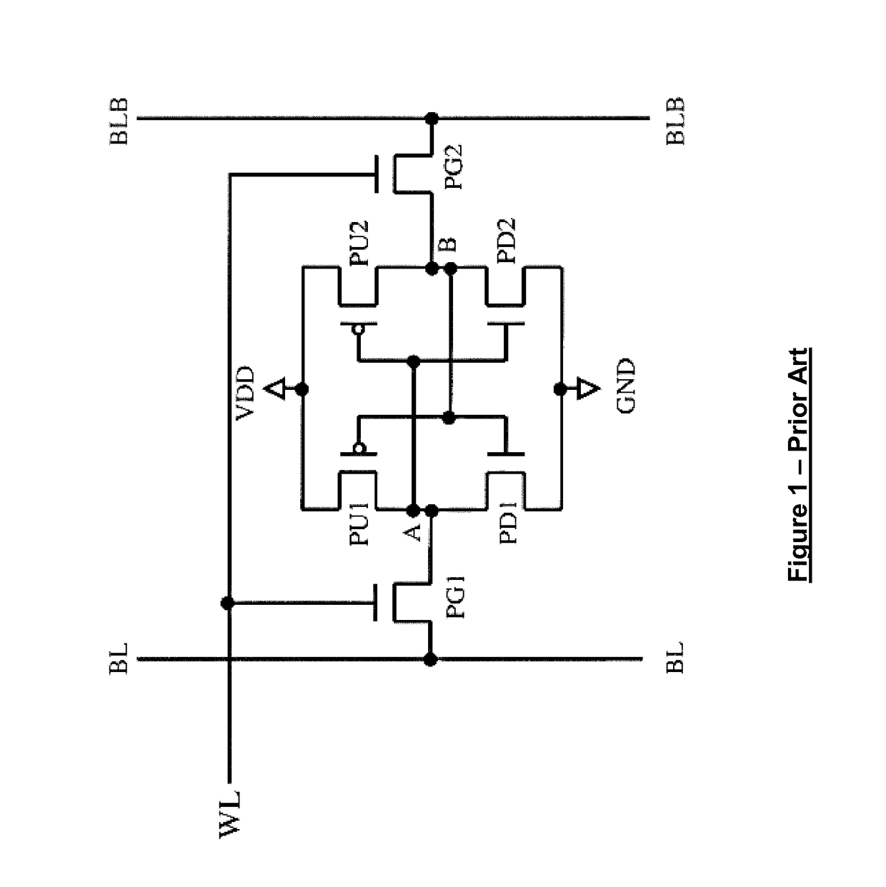
[0018]FIG. 1 illustrates a circuit diagram of an exemplary conventional six transistor (6T) static random access memory (SRAM) bitcell;

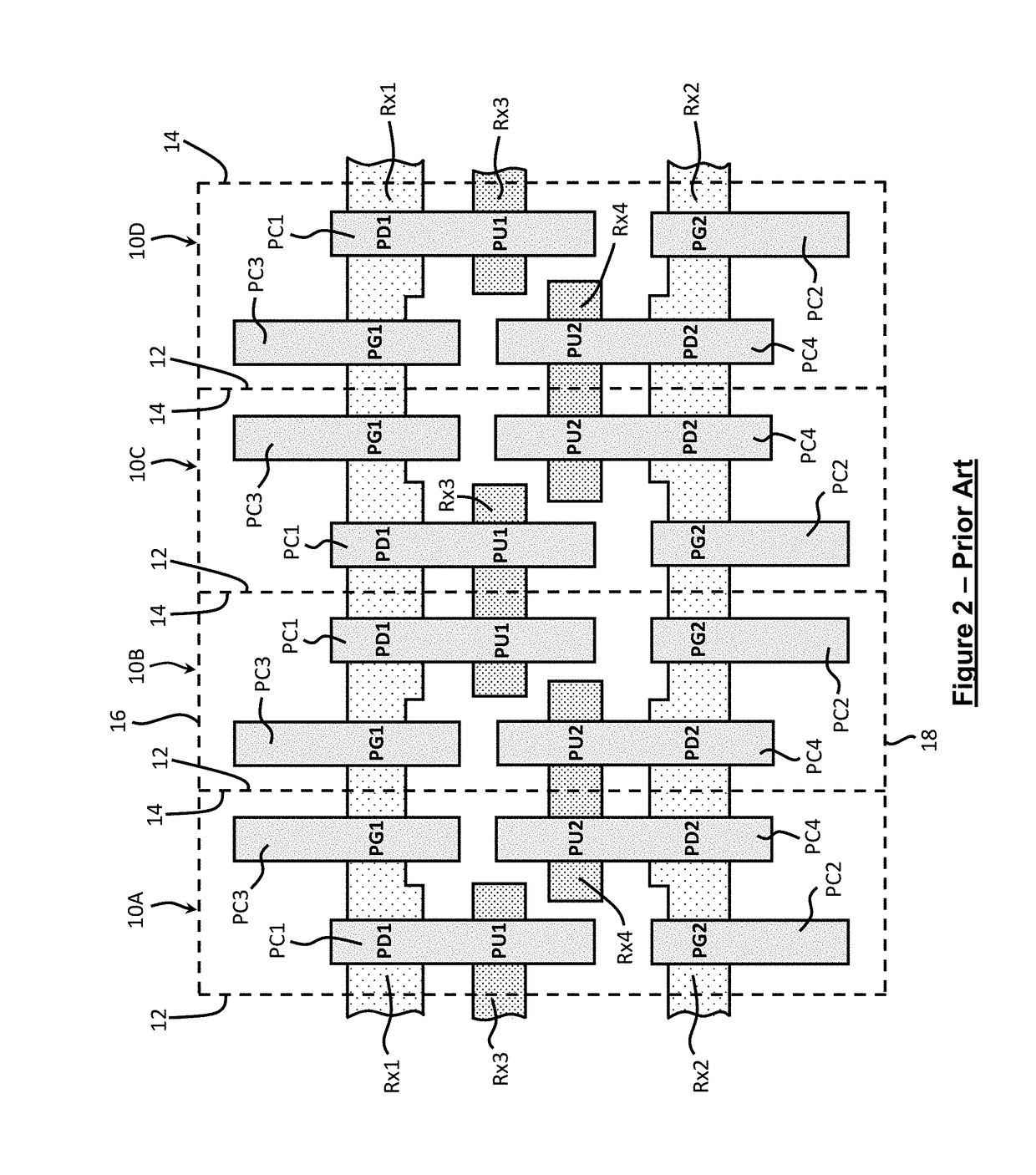
[0019]FIG. 2 illustrates a top view of an exemplary array of the exemplary 6T SRAM bitcell shown in FIG. 1;

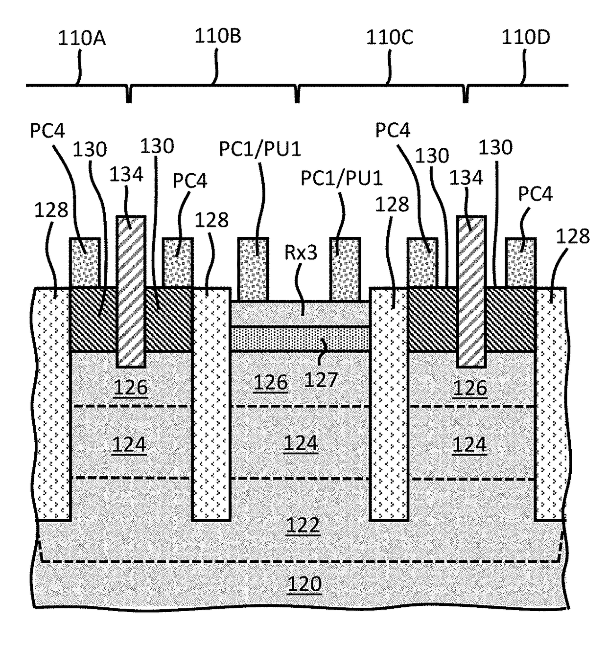
[0020]FIG. 3 illustrates an exemplary array of exemplary 6T SRAM bitcells fabricated on a SOI substrate according to the present disclosure;

[0021]FIG. 4 illustrates a cross-sectional...


PUM


Abstract

Static random access memory (SRAM) bitcell structures with improved minimum operation voltage (Vmin) and yield are provided. The structures may include a silicon substrate, a deep n-well (DNW) layer, p-well (PW) regions, doped back-plate (BP) regions, a buried oxide (BOX) layer, and / or active regions formed on the BOX layer and over portions of the BP regions. At least one BP region may extend below at least one shallow trench isolation (STI) region, at least one contact to back plate (CBP), at least one active region and at least one PC construct overlapping the at least one active region forming a channel of at least one of a first pass gate (PG1) transistor and a second pass gate (PG2) transistor. The at least one CBP facilitates biasing of at least one the PG1 and PG2 transistors during at least one of a read, write or standby operation of the structures.

Description

FIELD OF THE INVENTION[0001]The present disclosure generally relates to static random access memory (SRAM) bitcells, and more particularly, to SRAM bitcells fabricated on a silicon-on-insulator (SOI) substrate having improved minimum operation voltage (Vmin) and yield via dynamic biasing of at least one pass gate transistor thereof.BACKGROUND OF THE INVENTION[0002]Static random access memory (SRAM) cells or bitcells are commonly used in integrated circuits as a type of semiconductor memory that uses bistable latching circuitry to store each bit. SRAM can be fabricated on a silicon-on-insulator (SOI) substrate or a bulk silicon substrate with substantially the same operation principles. The term static differentiates it from dynamic RAM which must be periodically refreshed. SRAM bitcells have the advantageous feature of holding data without requiring a refresh. Some SRAM bitcells are single port, while some other SRAM bitcells are dual port. One typical SRAM bitcell is made up of six...

Claims


Application Information

Patent Timeline
Patent Type & Authority Patents(United States)
IPC IPC(8): G11C11/00H01L21/762H01L23/522H01L27/11G11C11/419G11C11/412
CPCG11C11/419H01L27/1104H01L23/5226H01L21/76224G11C11/412H01L27/11H01L27/0207H10B10/12H10B10/00
Inventor ZANG, HUIELLER, MANFREDCHI, MIN-HWA
Owner GLOBALFOUNDRIES US INC
Features
  • R&D
  • Intellectual Property
  • Life Sciences
  • Materials
  • Tech Scout
  • Unparalleled Data Quality
  • Higher Quality Content
  • 60% Fewer Hallucinations
Learn More