Semiconductor devices with varying threshold voltage and fabrication methods thereof

a technology of threshold voltage and semiconductor, applied in the direction of semiconductor devices, electrical equipment, transistors, etc., can solve the problems of increased system cost, increased system footprint, and increased system complexity

Active Publication Date: 2017-08-29
GLOBALFOUNDRIES US INC
View PDF8 Cites 324 Cited by
  • Summary
  • Abstract
  • Description
  • Claims
  • Application Information

AI Technical Summary

Benefits of technology

[0003]Certain shortcomings of the prior art can be overcome and additional advantages can be provided through the provision, in one aspect, of a method for fabricating a semiconductor device including, for instance, providing a structure with at least one region and including a dielectric layer disposed over a substrate; forming a multilayer stack structure including a threshold-voltage adjusting layer over the dielectric layer, the multilayer stack structure including a first threshold-voltage adjusting layer in

Problems solved by technology

A system using multiple discrete devices, each optimized for different functions, will

Method used


Image

  • Semiconductor devices with varying threshold voltage and fabrication methods thereof
  • Semiconductor devices with varying threshold voltage and fabrication methods thereof
  • Semiconductor devices with varying threshold voltage and fabrication methods thereof

Examples


Embodiment Construction

[0016]Aspects of the present invention and certain features, advantages, and details thereof, are explained more fully below with reference to the non-limiting examples illustrated in the accompanying drawings. Descriptions of well-known materials, fabrication tools, processing techniques, etc., are omitted so as not to unnecessarily obscure the invention in details. It should be understood, however, that the detailed description and the specific examples, while indicating embodiments of the invention, are given by way of illustration only, and not by way of limitation. Various substitutions, modifications, additions and / or arrangements within the spirit and / or scope of the underlying inventive concepts will be apparent to those skilled in the art from this disclosure.

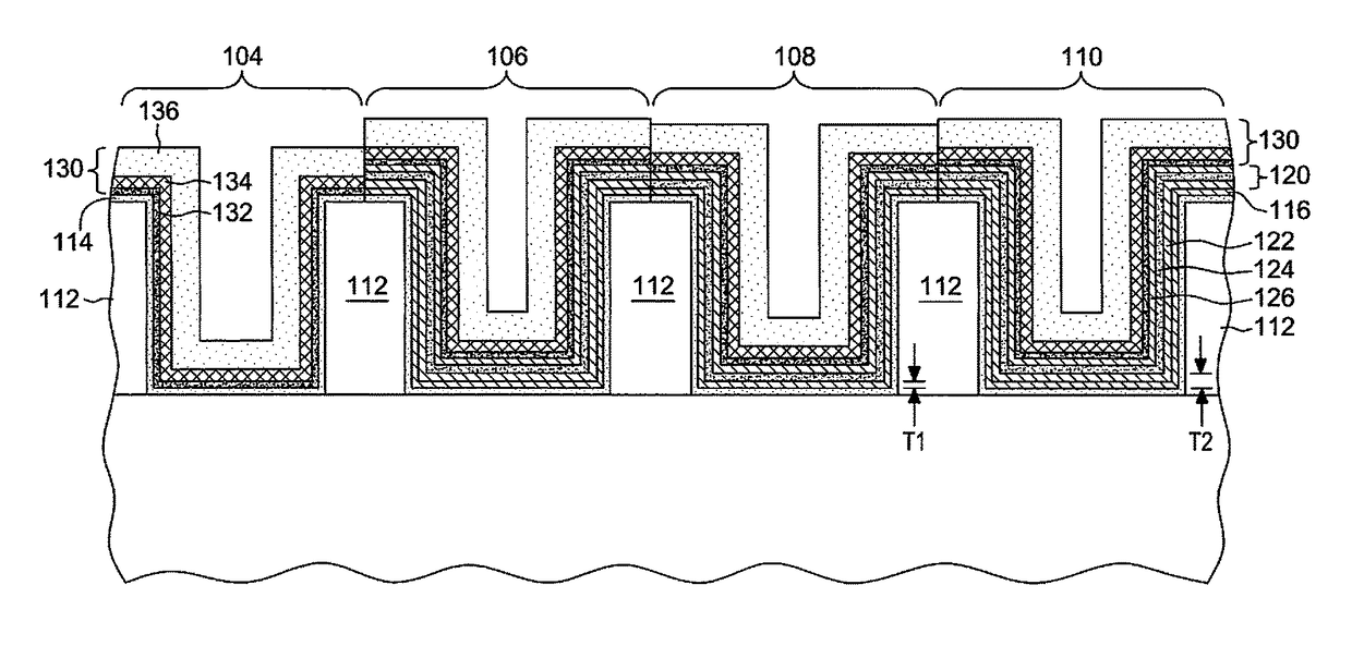
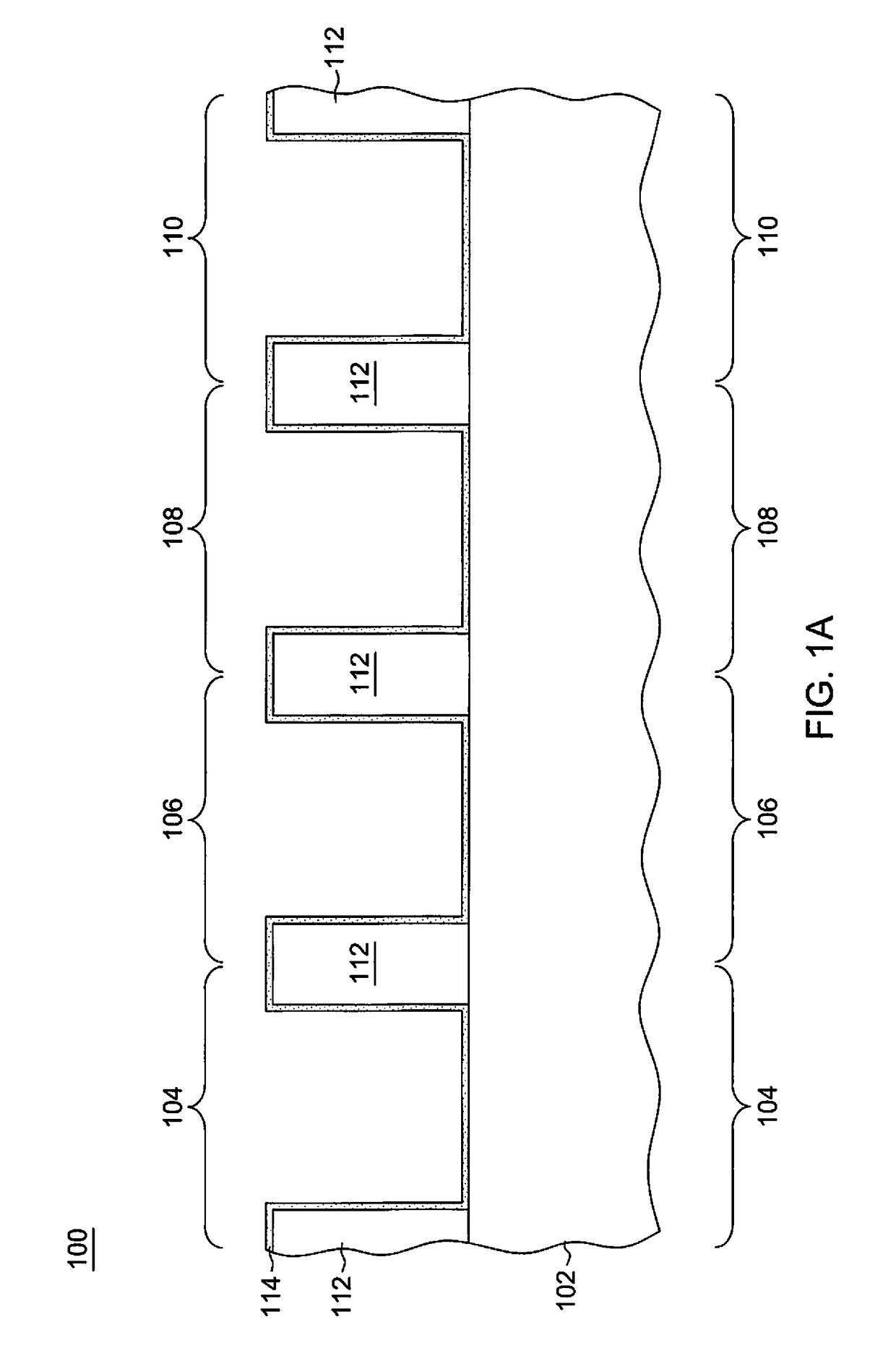
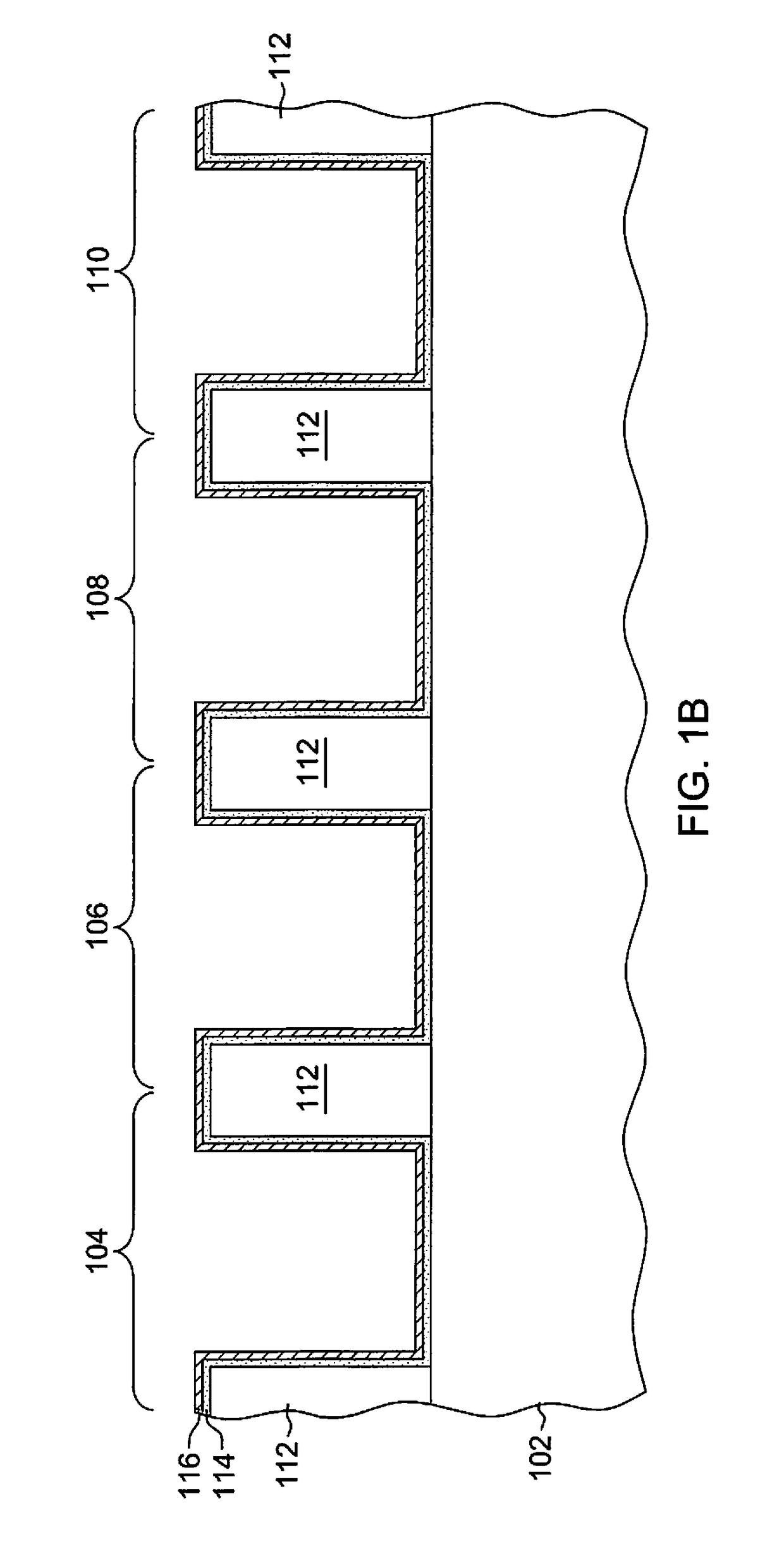
[0017]The present invention provides, in part, a method for fabricating a semiconductor device(s), including field-effect transistor (FETs) devices having varying threshold voltages. In one aspect and in a typical inte...


PUM


Abstract

Semiconductor device fabrication methods are provided which include: providing a structure with at least one region and including a dielectric layer disposed over a substrate; forming a multilayer stack structure including a threshold-voltage adjusting layer over the dielectric layer, the multilayer stack structure including a first threshold-voltage adjusting layer in a first region of the at least one region, and a second threshold-voltage adjusting layer in a second region of the at least one region; and annealing the structure to define a varying threshold voltage of the at least one region, the annealing facilitating diffusion of at least one threshold voltage adjusting species from the first threshold-voltage adjusting layer and the second threshold-voltage adjusting layer into the dielectric layer, where a threshold voltage of the first region is independent of the threshold voltage of the second region.

Description

FIELD OF THE INVENTION[0001]The present invention relates to semiconductor devices and methods for fabricating the semiconductor devices, and more particularly, to semiconductor devices with varying threshold voltages.Background[0002]Different semiconductor devices are traditionally fabricated to have one or more different device characteristics, such as threshold voltage, switching speed, leakage power consumption, etc. Multiple different designs may each provide optimization of one or more of these characteristics for devices intended to perform specific functions. For instance, one design may have reduced threshold voltage to increase switching speed for devices providing computational logic functions, and another design may have increased threshold voltage to decrease power consumption for devices providing memory storage functions. As is known in semiconductor device technology, such as, field-effect transistors (FETs), the threshold voltage is the minimum gate voltage required...

Claims


Application Information

Patent Timeline
IPC IPC(8): H01L21/8238H01L21/324H01L21/225H01L29/66H01L27/092
CPCH01L21/823807H01L21/324H01L21/823828H01L21/2254H01L29/66545H01L27/092H01L21/823842H01L21/823857H01L29/4966H01L29/517H01L29/518
Inventor KANNAN, BALAJIKWON, UNOHKRISHNAN, SIDDARTHANDO, TAKASHINARAYANAN, VIJAY
Owner GLOBALFOUNDRIES US INC
Why Eureka
Try Eureka