Semiconductor device and method for manufacturing the semiconductor device

a semiconductor and semiconductor technology, applied in the direction of semiconductor devices, semiconductor/solid-state device details, electrical apparatus, etc., can solve the problems of difficult to increase the number of al wires, and melted al wires, etc., to prevent the occurrence of cracks in the wires, improve the hardness, and strengthen the electrodes

Active Publication Date: 2017-08-29
FUJI ELECTRIC CO LTD
View PDF17 Cites 0 Cited by
  • Summary
  • Abstract
  • Description
  • Claims
  • Application Information

AI Technical Summary

Benefits of technology

[0023]According to the invention, the recrystallization temperature of the wire is higher than the recrystallization temperature of the aluminum wire according to the related art. Therefore, it is possible to prevent the occurrence of cracks in the wire even under the usage conditions at a temperature higher than that in the related art. As a result, the period until cracks occur in the wire can be longer than that in the related art.
[0024]According to the invention, the metal film with a higher hardness than the wire is provided on the surface of the electrode of the semiconductor element (semiconductor chip) to strengthen the electrode. Therefore, it is possible to prevent the occurrence of cracks in the electrode. In addition, the metal film with a higher hardness than the wire is provided on the surface of the electrode and functions as a protective wall. Therefore, even when cracks occur in the wire, it is possible to prevent the extension of the cracks to the electrode.
[0025]According to the semiconductor device and the method for manufacturing a semiconductor device of the invention, it is possible to improve power cycle resistance.

Problems solved by technology

Therefore, it is difficult to increase the number of Al wires in order to increase the amount of current and there is a concern that the Al wire will be melted and broken due to the generation of heat from the wire when a large amount of current flows to each Al wire.
As a result, there is a concern that the element will be broken.
As a result, a crack (breaking) is likely to occur in the vicinity of the bonding interface between the Al wire and the top side electrode.
The inventors performed the power cycle test and found that cracks occurred in the Al wire and extended to the inside of the wire with an increase in the number of power cycles, and the Al wire was finally broken and detached, which resulted in the breakdown of the element.

Method used


Image

  • Semiconductor device and method for manufacturing the semiconductor device
  • Semiconductor device and method for manufacturing the semiconductor device
  • Semiconductor device and method for manufacturing the semiconductor device

Examples


embodiments

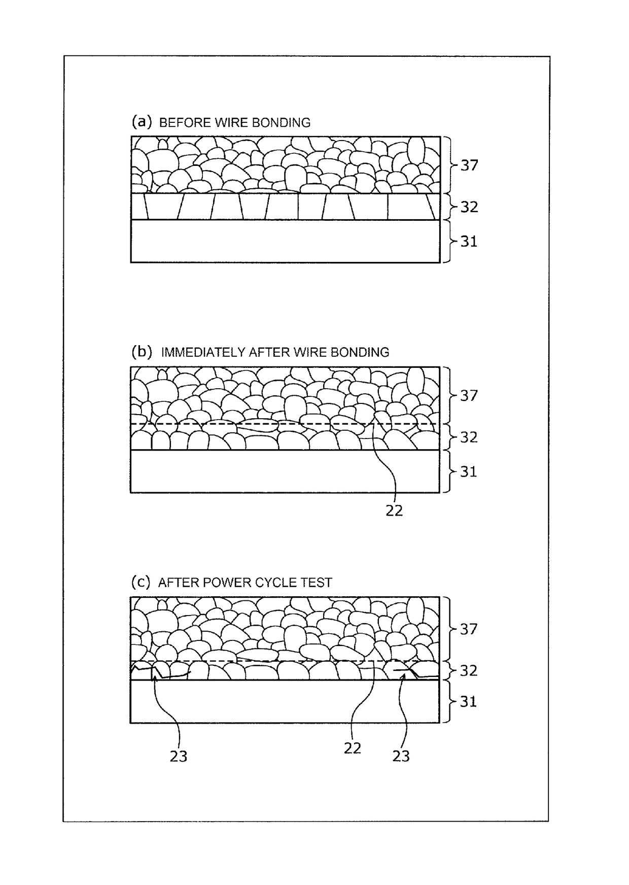
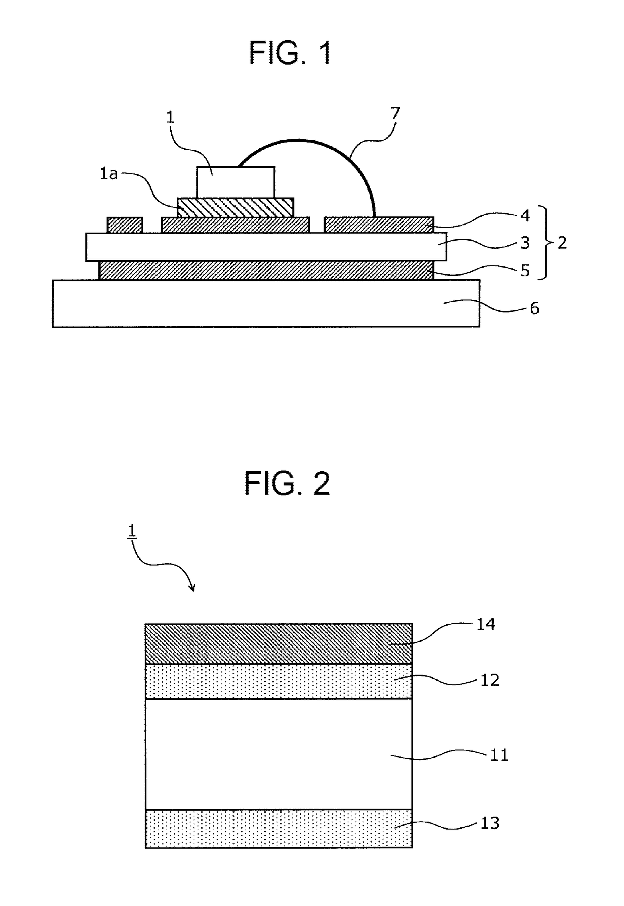
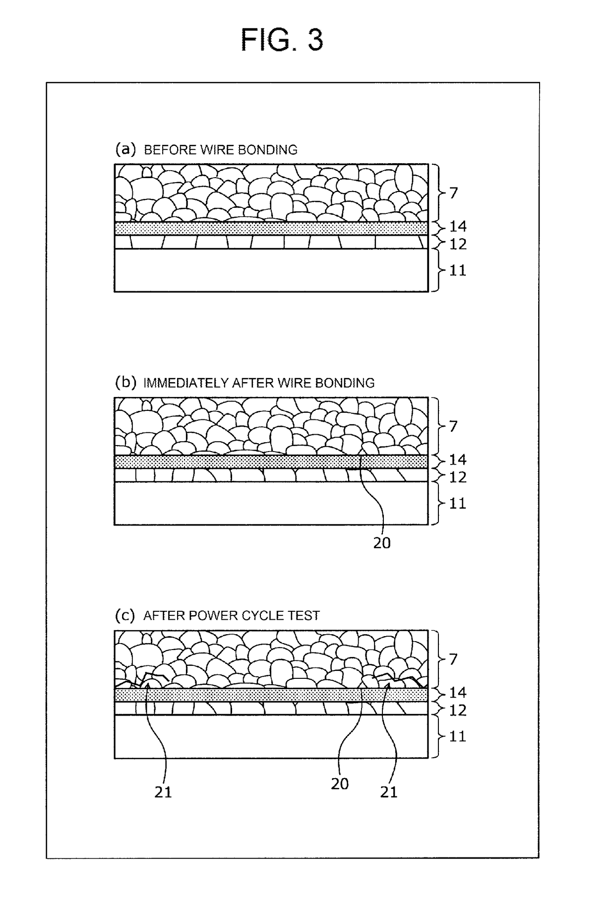
[0041]The structure of a semiconductor device according to an embodiment will be described. FIG. 1 is a cross-sectional view illustrating the structure of the semiconductor device according to the embodiment. FIG. 2 is a cross-sectional view schematically illustrating the structure of a semiconductor element illustrated in FIG. 1. As illustrated in FIGS. 1 and 2, the semiconductor device according to the embodiment has a module structure including a semiconductor element (semiconductor chip) 1, an insulated substrate 2, such as a ceramics insulated substrate (DCB substrate), a copper (Cu) base 6, and a wire 7. In the insulated substrate 2, a circuit layer 4 which is made of, for example, Cu is provided on the front surface of an insulated layer 3 and a copper layer 5 is provided on the rear surface of the insulated layer 3.

[0042]The semiconductor element 1 includes a top side electrode 12 which is provided on the front surface of a semiconductor die (for example, a silicon (Si) subs...


PUM

PropertyMeasurementUnit
bonding temperatureaaaaaaaaaa
grain sizeaaaaaaaaaa
thicknessaaaaaaaaaa

Abstract

A semiconductor device has a module structure in which a semiconductor element and a circuit layer are electrically connected to each other by a wire. A front metal layer is formed on a surface of a top side electrode of the semiconductor element and the wire is bonded to the front metal layer by wire bonding. The front metal layer has a higher hardness than the top side electrode or the wire. A bonding interface of the wire with the metal film has a recrystallization temperature that is equal to or higher than 175° C. According to this structure, it is possible to improve the power cycle resistance of the semiconductor device.

Description

CROSS-REFERENCE TO RELATED APPLICATION(S)[0001]This non-provisional application for a U.S. Patent is a Continuation of International Application PCT / JP2014 / 061457 filed Apr. 23, 2014, which claims priority from JP PA 2013-092110 filed Apr. 25, 2013, the entire contents of both of which are hereby incorporated by reference.BACKGROUND OF THE INVENTION[0002]1. Field of the Invention[0003]The present invention relates to a semiconductor device and a method for manufacturing the semiconductor device.[0004]2. Background of the Related Art[0005]A method has been known which electrically connects (bonds) a top side electrode of a semiconductor element and a circuit layer with a wire, such as an aluminum (Al) wire, in a semiconductor device with a module structure that is used in, for example, a general-purpose inverter, a wind power generation system, a photovoltaic generation system, and an electric railroad. The top side electrode is, for example, an aluminum-silicon (Si) electrode or an ...

Claims


Application Information

Patent Timeline
Patent Type & Authority Patents(United States)
IPC IPC(8): H01L23/48H01L23/00
CPCH01L24/05H01L24/03H01L24/43H01L24/45H01L24/48H01L24/73H01L24/85H01L2224/48855H01L2224/73265H01L2224/85H01L2224/85203H01L2224/85205H01L2924/2064H01L24/29H01L2224/04042H01L2224/05124H01L2224/05541H01L2224/05624H01L2224/05647H01L2224/05655H01L2224/29101H01L2224/32225H01L2224/45124H01L2224/45147H01L2224/4851H01L2224/48091H01L2224/48227H01L2224/48724H01L2224/48747H01L2224/48755H01L2224/48824H01L2224/48847H01L2924/00014H01L2924/00H01L2924/01014H01L2924/01029H01L2924/01026H01L2924/0104H01L2924/01204H01L2924/013H01L2924/00015H01L2924/014H01L2224/45015H01L2924/2075H01L2924/20751H01L2924/20752H01L2924/20753H01L2924/20754H01L2924/20755H01L2924/20756H01L2924/20757H01L2924/20758H01L2924/20759H01L2924/2076H01L2924/00012
Inventor MOMOSE, FUMIHIKOSAITO, TAKASHIKIDO, KAZUMASANISHIMURA, YOSHITAKA
Owner FUJI ELECTRIC CO LTD
Why Eureka
Try Eureka