Printing high aspect ratio patterns

a high aspect ratio, pattern technology, applied in the direction of conductive pattern formation, printed circuit stress/warp reduction, thermography, etc., can solve the problems of printed pattern distortion so as to facilitate the accurate placement of the second and complicate the second printed layer registration

Active Publication Date: 2017-08-29
WUHAN DR LASER TECH CORP LTD
View PDF9 Cites 4 Cited by
  • Summary
  • Abstract
  • Description
  • Claims
  • Application Information

AI Technical Summary

Benefits of technology

[0008]Dispensing the paste and printing the pattern “wet-on-wet” facilitates accurate placement of the second and additional paste layers, since thermal processing of the printed layer, for example drying of the paste, would inevitably generate printed pattern distortions and complicate the second printed layer registration. The wet-on-wet printing process is free of this drawback.

Problems solved by technology

Dispensing the paste and printing the pattern “wet-on-wet” facilitates accurate placement of the second and additional paste layers, since thermal processing of the printed layer, for example drying of the paste, would inevitably generate printed pattern distortions and complicate the second printed layer registration.

Method used


Image

  • Printing high aspect ratio patterns
  • Printing high aspect ratio patterns
  • Printing high aspect ratio patterns

Examples


Embodiment Construction

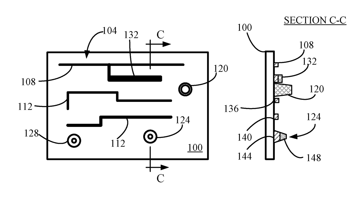
[0016]The ability to print high aspect ratio patterns and in particular patterns including electrically conductive patterns could support the combination of thinner, higher signal conducting conductors or tracks and thicker electric power supplying conductors or tracks printed on the same substrate. Different components could be mounted or connected to segments with different segment thickness. Segments with different segment thickness could increase the packaging density, improve thermal dissipation, lower electronic circuit assembly costs, reduce the number of interconnections and improve the product reliability.

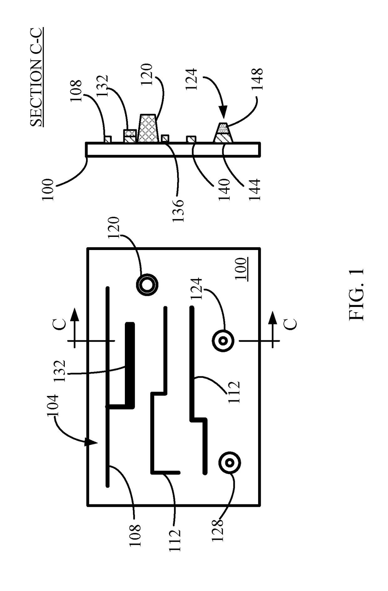
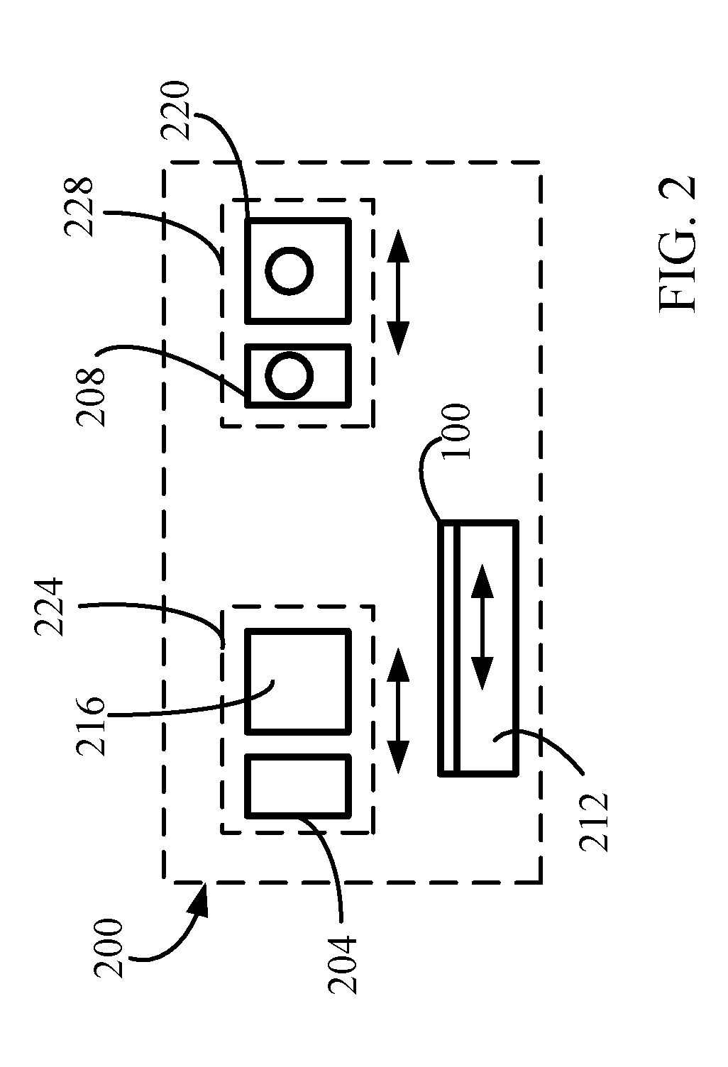
[0017]Reference is made to FIG. 1, which is a schematic illustration of an example of a substrate with a printed on it pattern including segments of different aspect ratio. Substrate 100 could include a pattern 104 of conductors or tracks 108, 112 and 116 and a number of pyramidal, conical, cylindrical or other cross section stubs 120, 124 and 128. Each conductor 108, 112,...


PUM

PropertyMeasurementUnit
thicknessaaaaaaaaaa
widthaaaaaaaaaa
aspect ratioaaaaaaaaaa

Abstract

Described are an apparatus and a method for printing a high aspect ratio and / or specific vertical geometry pattern. The apparatus operates in a multi-pass printing mode and includes one or more paste dispensing mechanism configured to dispense a high viscosity paste to form a pattern on a substrate. At least one paste dispensing mechanism is configured to dispense the paste to a segment of the pattern printed at an earlier pass. The paste is dispensed to the relevant segment of the pattern earlier printed before the paste printed at the earlier made pass is dry or what is termed “wet-on-wet” printing.

Description

TECHNOLOGY FIELD[0001]The apparatus and method relate to the field of printed electronics and in particular to printing high aspect ratio patterns of conductors and components.BACKGROUND[0002]Printed electronics is a novel recently developed electronics production method. It is a relatively low cost production method allowing flexible placement of passive and active electronic components including resistor, capacitors, inductors and electrical current conductors or simply conductors. Different materials in paste form are used to vary properties such as for example resistance, of the printed conductors and printed components.[0003]One of the primary printing methods for producing conductive patterns on different types of substrates, particularly for features larger than about 100 microns, is screen printing. In screen printing a paste is squeezed through a stencil bearing the desired pattern. When conductive patterns are printed the paste can contain metal particles, such as silver a...

Claims


Application Information

Patent Timeline
Patent Type & Authority Patents(United States)
IPC IPC(8): H05K3/12B41M5/26C09D17/00H05K1/09B41M3/00H05K1/02
CPCH05K3/12B41M5/26C09D17/00H05K1/0271H05K1/095B41M3/008H05K1/0265H05K2201/09736H05K2203/107H05K2203/1476
Inventor NOY, AMIR
Owner WUHAN DR LASER TECH CORP LTD
Why Eureka
Try Eureka