Semiconductor device and electronic device

a semiconductor and electronic technology, applied in the field of semiconductor devices, can solve the problems of increasing power consumption, image processing is executed while consuming a large quantity of power, etc., and achieve the effects of high speed, high resolution, and high-integration of semiconductor devices

Inactive Publication Date: 2017-09-26
SEMICON ENERGY LAB CO LTD
View PDF153 Cites 22 Cited by
  • Summary
  • Abstract
  • Description
  • Claims
  • Application Information

AI Technical Summary

Benefits of technology

[0017]In the above procedure, data is read from and stored in the digital memory frequently; thus, the increase in arithmetic processing speed is required. Note that the arithmetic processing time can be shortened when a plurality of multiplication circuits or a plurality of addition circuits are provided to perform parallel processing. However, processing with such a structure increases power consumption.
[0018]An object of one embodiment of the present invention is to provide a semiconductor device with an image processing function. Another object of one embodiment of the present invention is to provide a semiconductor device capable of outputting data subjected to image processing. Another object of one embodiment of the present invention is to provide a low-power semiconductor device. Another object of one embodiment of the present invention is to provide a semiconductor device that is suitable for high-speed operation. Another object of one embodiment of the present invention is to provide a semiconductor device with high resolution. Another object of one embodiment of the present invention is to provide a highly integrated semiconductor device. Another object of one embodiment of the present invention is to provide a semiconductor device capable of imaging under a low illuminance condition. Another object of one embodiment of the present invention is to provide a semiconductor device with a wide dynamic range. Another object of one embodiment of the present invention is to provide a semiconductor device that can be used in a wide temperature range. Another object of one embodiment of the present invention is to provide a semiconductor device with a high aperture ratio. Another object of one embodiment of the present invention is to provide a semiconductor device with high reliability.
[0019]Another object of one embodiment of the present invention is to provide a semiconductor device with an arithmetic processing function. Another object of one embodiment of the present invention is to provide a semiconductor device capable of outputting data subjected to arithmetic processing. Another object of one embodiment of the present invention is to provide a semiconductor device including a memory element with excellent retention performance. Another object of one embodiment of the present invention is to provide a semiconductor device including a memory element with excellent write performance. Another object of one embodiment of the present invention is to provide a semiconductor device including a highly integrated memory element. Another object of one embodiment of the present invention is to provide a semiconductor device including a memory element with high capacity. Another object of one embodiment of the present invention is to provide a semiconductor device including a highly reliable memory element. Another object of one embodiment of the present invention is to provide a semiconductor device or the like including a novel memory element. Another object of one embodiment of the present invention is to provide a novel semiconductor device or the like.
[0036]According to one embodiment of the present invention, a semiconductor device with an image processing function can be provided. A semiconductor device capable of outputting data subjected to image processing can be provided. A low-power semiconductor device can be provided. A semiconductor device that is suitable for high-speed operation can be provided. A semiconductor device with high resolution can be provided. A highly integrated semiconductor device can be provided. A semiconductor device capable of imaging under a low illuminance condition can be provided. A semiconductor device with a wide dynamic range can be provided. A semiconductor device that can be used in a wide temperature range can be provided. A semiconductor device with a high aperture ratio can be provided. A semiconductor device with high reliability can be provided.
[0037]A semiconductor device with an arithmetic processing function can be provided. A semiconductor device capable of outputting data subjected to arithmetic processing can be provided. A semiconductor device including a memory element with excellent retention performance can be provided. A semiconductor device including a memory element with excellent write performance can be provided. A semiconductor device including a highly integrated memory element can be provided. A semiconductor device including a memory element with high capacity can be provided. A semiconductor device including a highly reliable memory element can be provided. A semiconductor device or the like including a novel memory element can be provided. A novel semiconductor device or the like can be provided.

Problems solved by technology

Therefore, image processing is executed while consuming a large quantity of power.
However, processing with such a structure increases power consumption.

Method used


Image

  • Semiconductor device and electronic device
  • Semiconductor device and electronic device
  • Semiconductor device and electronic device

Examples


embodiment 1

(Embodiment 1)

[0096]In this embodiment, an imaging device that is one embodiment of the present invention is described with reference to drawings.

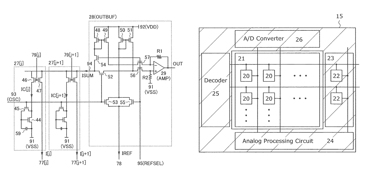
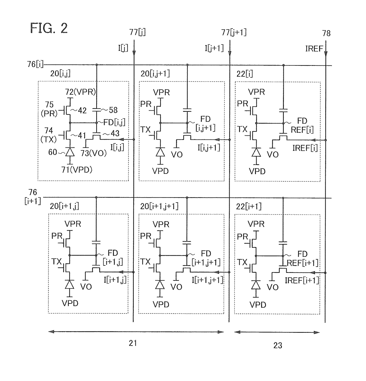
[0097]FIG. 1 is a block diagram illustrating an imaging device in one embodiment of the present invention. The imaging device includes a pixel array 21 where pixels 20 for imaging are arranged in a matrix, a reference pixel array 23 where reference pixels 22 for image processing are arranged, an analog processing circuit 24, and a row decoder 25 that outputs a potential for image processing to each pixel. Note that an A / D converter 26 can be used when image processing is not performed. Thus, the A / D converter 26 can be omitted.

[0098]Although the pixel array 21 and the reference pixel array 23 are separately illustrated, circuits of the pixels 20 and the reference pixels 22 have the same structure. Therefore, in the plurality of pixels arranged in a matrix, the pixels in one column at an end function as the reference pixel array 23, and the...

embodiment 2

(Embodiment 2)

[0228]In this embodiment, a semiconductor device including a memory element in one embodiment of the present invention is described with reference to drawings. The semiconductor device including a memory element in one embodiment of the present invention can perform vector matrix multiplication. The vector matrix multiplication is, for example, operation frequently used in an arithmetic processing unit, such as smoothing processing, edge enhancement processing, or cosine transform in image processing.

[0229]FIG. 25 is a block diagram illustrating a semiconductor device in one embodiment of the present invention. The semiconductor device includes a memory element array 521 where memory elements 520 are arranged in a matrix, a reference memory element array 523 where reference memory elements 522 for arithmetic processing are arranged, an analog processing circuit 524, and a row decoder 525 that outputs a potential for writing or reading to the memory element 520 and the ...

embodiment 3

(Embodiment 3)

[0307]In this embodiment, a transistor including an oxide semiconductor that can be used in one embodiment of the present invention is described with reference to drawings. In the drawings in this embodiment, some components are enlarged, reduced in size, or omitted for easy understanding.

[0308]FIGS. 33A and 33B are a top view and a cross-sectional view illustrating a transistor 101 in one embodiment of the present invention. FIG. 33A is a top view, and a cross section in the direction of dashed-dotted line B1-B2 in FIG. 33A is illustrated in FIG. 33B. A cross section in the direction of dashed-dotted line B3-B4 in FIG. 33A is illustrated in FIG. 35A. The direction of dashed-dotted line B1-B2 is referred to as a channel length direction, and the direction of dashed-dotted line B3-B4 is referred to as a channel width direction.

[0309]The transistor 101 includes an insulating layer 120 in contact with a substrate 115; an oxide semiconductor layer 130 in contact with the i...


PUM


Abstract

A semiconductor device including pixels arranged in a matrix of n rows and m columns, in which the pixels in the m-th column are shielded from light, is provided.

Description

BACKGROUND OF THE INVENTION[0001]1. Field of the Invention[0002]One embodiment of the present invention relates to a semiconductor device including an oxide semiconductor.[0003]Note that one embodiment of the present invention is not limited to the above technical field. The technical field of one embodiment of the invention disclosed in this specification and the like relates to an object, a method, or a manufacturing method. One embodiment of the present invention relates to a process, a machine, manufacture, or a composition of matter. Specifically, examples of the technical field of one embodiment of the present invention disclosed in this specification include a semiconductor device, a display device, a liquid crystal display device, a light-emitting device, a lighting device, a power storage device, a storage device, an imaging device, a method for driving any of them, and a method for manufacturing any of them.[0004]In this specification and the like, a semiconductor device g...

Claims


Application Information

Patent Timeline
Patent Type & Authority Patents(United States)
IPC IPC(8): H01L27/146H01L29/24H01L31/0272H01L31/032
CPCH01L27/14643H01L27/14609H01L27/14612H01L27/14623H01L27/14636H01L27/14667H01L29/24H01L31/0272H01L31/0322Y02E10/541Y02P70/50
Inventor KUROKAWA, YOSHIYUKI
Owner SEMICON ENERGY LAB CO LTD
Why Eureka
Try Eureka