Supercharge Your Innovation With Domain-Expert AI Agents!

Self-aligned pitch split for unidirectional metal wiring

a self-aligned, metal wiring technology, applied in the direction of electrical equipment, semiconductor devices, semiconductor/solid-state device details, etc., can solve the problems of difficult control of overlay, difficult to cut away features at tight pitch, and many pattern constructs cannot be drawn directly

Active Publication Date: 2017-10-10
INT BUSINESS MASCH CORP
View PDF15 Cites 7 Cited by
  • Summary
  • Abstract
  • Description
  • Claims
  • Application Information

AI Technical Summary

Benefits of technology

The present invention provides a method for creating metal wiring on a wafer using a hybrid approach. The method includes forming a copper layer on the wafer, adding a patterned hardmask to the copper layer, and then using the hardmask to create a pattern of copper lines on the wafer. Extra coating is applied to fill the spaces between the first copper lines. The method also includes etching trenches in the extra coating and then filling them with copper to create self-aligned second copper lines. This technique allows for precise placement of copper lines, reducing the risk of short-circuiting and other issues. The invention also provides an electronic device with the metal wiring layer mentioned above.

Problems solved by technology

A disadvantage of using SIT processes is that many pattern constructs can not be drawn directly (for example, an odd number of lines, or two parallel lines which do not connect), necessitating a trim process to remove unwanted features.
Trimming away features at tight pitch without removing desired features is extremely challenging, requiring excellent overlay tolerance of the trim mask to the SIT patterns, as well as excellent control over the dimension of the mandrel, which controls the exact placement of the SIT patterns.
In practice, controlling the overlay is difficult.

Method used


Image

  • Self-aligned pitch split for unidirectional metal wiring
  • Self-aligned pitch split for unidirectional metal wiring
  • Self-aligned pitch split for unidirectional metal wiring

Examples


Embodiment Construction

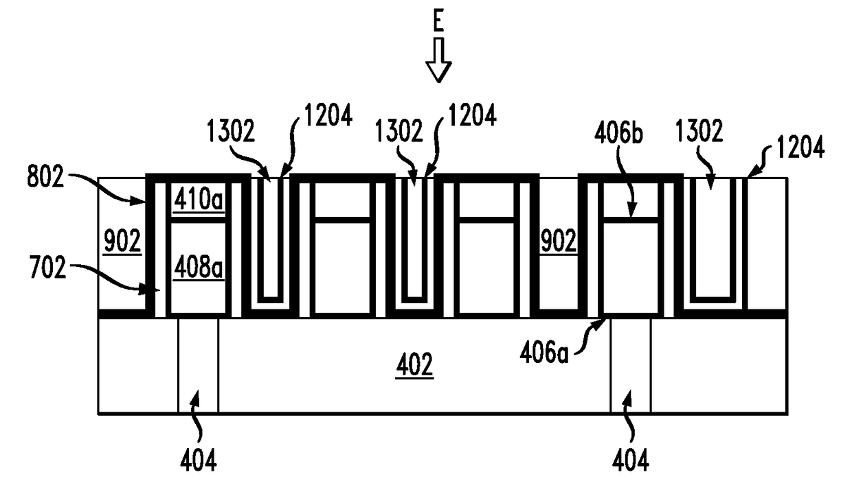
[0027]Provided herein are pitch split lithography techniques in which metal wiring at sublithographic pitch (beyond the 14 nanometer (nm) node—see above) is achieved using a hybrid metallization approach. Specifically, a first set of metal wiring is subtractively patterned, and then a second set of metal wiring is patterned using a damascene process which is self-aligned to the first set of wires in regions of minimum pitch. This subtractively patterned / damascene process is what is being referred to herein as a hybrid metallization approach. It is notable that while the present description illustrates embodiments that involve patterning of unidirectional metal wiring, this is merely one exemplary implementation of the present techniques. The process described herein may be applied to scenarios involving arbitrary wiring orientation.

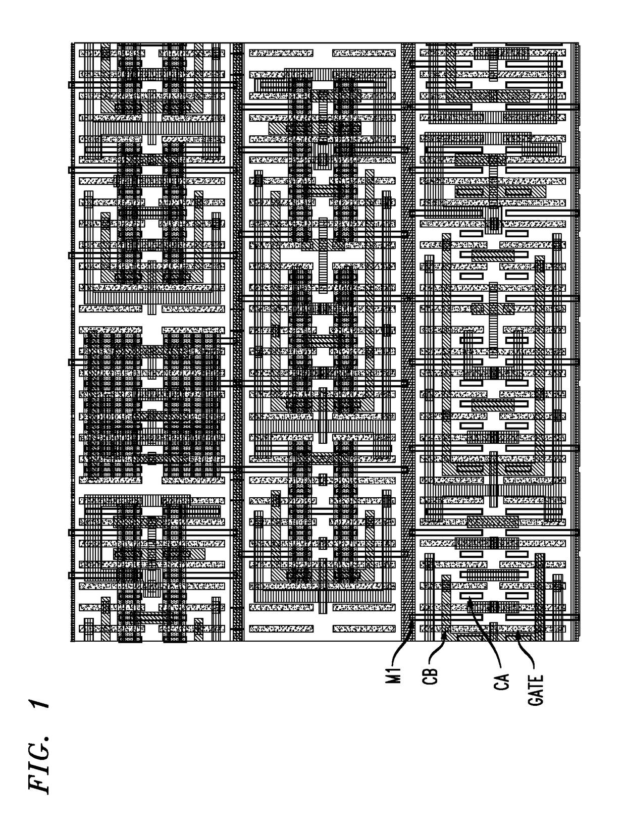
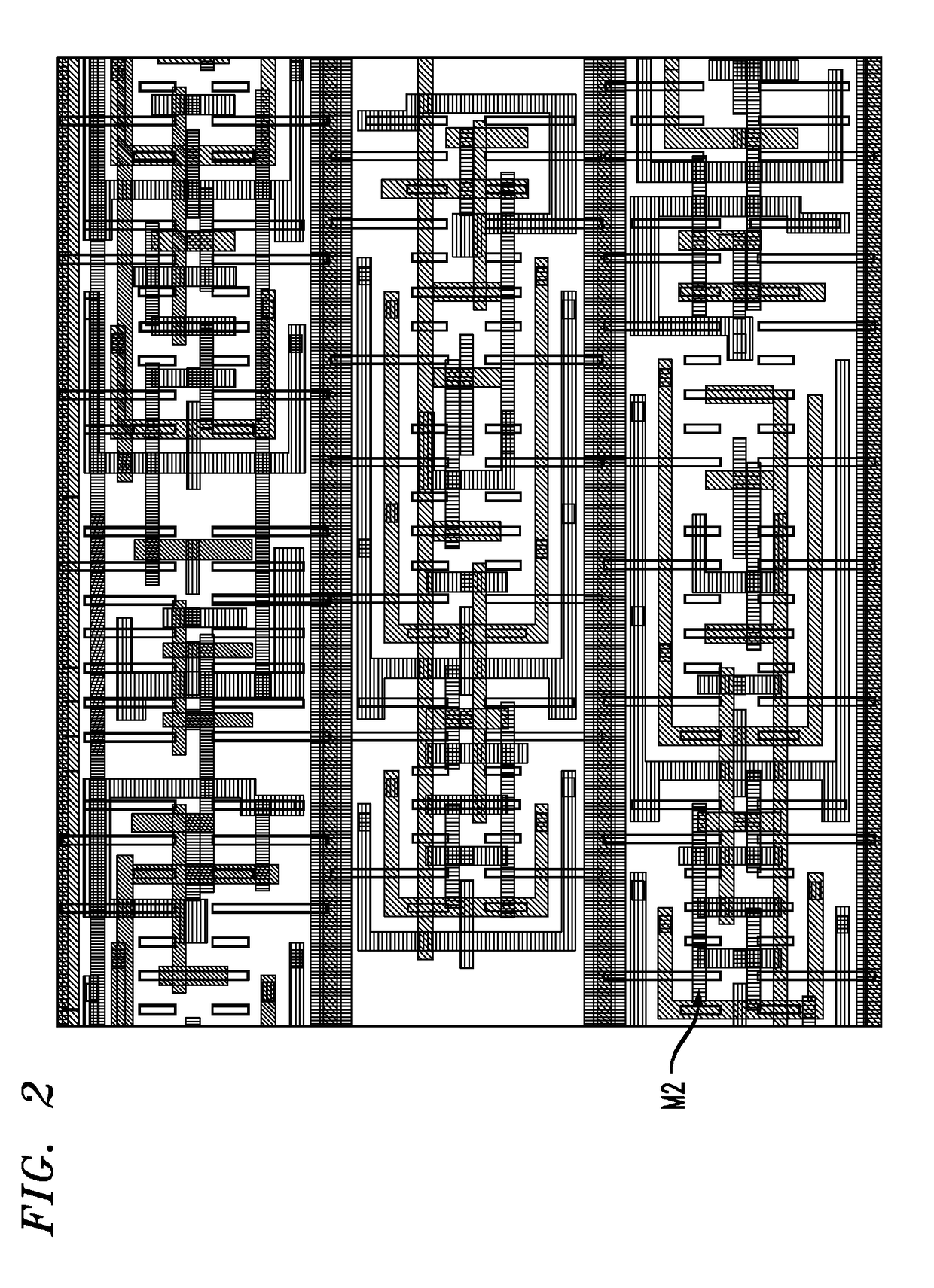
[0028]An overview of the present techniques is now provided by way of reference to FIGS. 1-3. In the example shown in FIGS. 1-3, the present techniques a...


PUM

PropertyMeasurementUnit
temperatureaaaaaaaaaa
dimensionaaaaaaaaaa
spacingaaaaaaaaaa

Abstract

Self-aligned pitch split techniques for metal wiring involving a hybrid (subtractive patterning / damascene) metallization approach are provided. In one aspect, a method for forming a metal wiring layer on a wafer includes the following steps. A copper layer is formed on the wafer. A patterned hardmask is formed on the copper layer. The copper layer is subtractively patterned using the patterned hardmask to form a plurality of first copper lines. Spacers are formed on opposite sides of the first copper lines. A planarizing dielectric material is deposited onto the wafer, filling spaces between the first copper lines. One or more trenches are etched in the planarizing dielectric material. The trenches are filled with copper to form a plurality of second copper lines that are self-aligned with the first copper lines. An electronic device is also provided.

Description

FIELD OF THE INVENTION[0001]The present invention relates to pitch split lithography techniques and more particularly, to self-aligned pitch split techniques for metal wiring involving a hybrid (subtractive patterning / damascene) metallization approach.BACKGROUND OF THE INVENTION[0002]For technology nodes beyond the 14 nanometer (nm) node the scaling roadmap dictates minimum wiring pitch which is smaller than that which can be printed with lithography techniques which are currently manufacturable, i.e., immersion 193 nm lithography. As advanced lithography techniques such as electron beam (e-beam), extreme UV, or directed self-assembly are not ready for manufacturing, the industry has resorted to so called “pitch split” techniques.[0003]One pitch split technique is sidewall image transfer (SIT), in which mandrel shapes are printed at double the target pitch, and each sidewall of the mandrel shapes is converted into a shape in the target material through a series of processes typicall...

Claims


Application Information

Patent Timeline
Patent Type & Authority Patents(United States)
IPC IPC(8): H01L23/528H01L23/48H01L21/768H01L23/532
CPCH01L23/528H01L21/76816H01L21/76832H01L21/76834H01L21/76841H01L21/76885H01L23/48H01L23/53238H01L2924/0002H01L21/76852H01L2924/00
Inventor CHANG, JOSEPHINE B.GUILLORN, MICHAEL A.JOSEPH, ERIC A.MIYAZOE, HIROYUKI
Owner INT BUSINESS MASCH CORP
Features
  • R&D
  • Intellectual Property
  • Life Sciences
  • Materials
  • Tech Scout
  • Unparalleled Data Quality
  • Higher Quality Content
  • 60% Fewer Hallucinations
Learn More